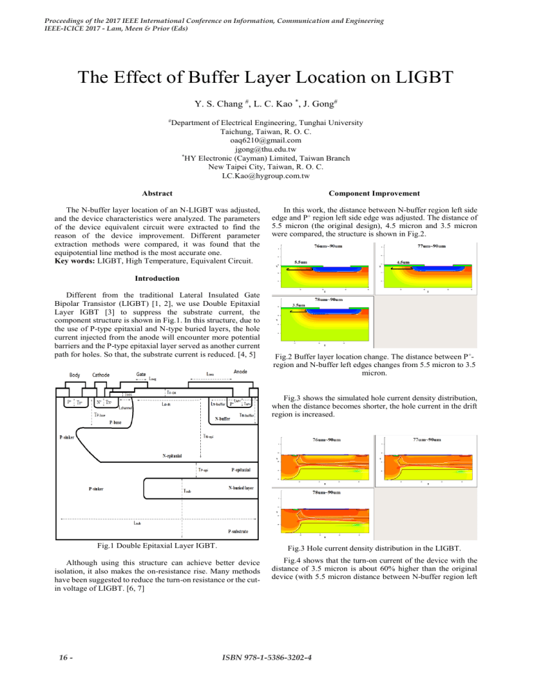
Proceedings of the 2017 IEEE International Conference on Information, Communication and Engineering IEEE-ICICE 2017 - Lam, Meen & Prior (Eds) The Effect of Buffer Layer Location on LIGBT Y. S. Chang #, L. C. Kao *, J. Gong# Department of Electrical Engineering, Tunghai University Taichung, Taiwan, R. O. C. oaq6210@gmail.com jgong@thu.edu.tw * HY Electronic (Cayman) Limited, Taiwan Branch New Taipei City, Taiwan, R. O. C. LC.Kao@hygroup.com.tw # Abstract Component Improvement The N-buffer layer location of an N-LIGBT was adjusted, and the device characteristics were analyzed. The parameters of the device equivalent circuit were extracted to find the reason of the device improvement. Different parameter extraction methods were compared, it was found that the equipotential line method is the most accurate one. Key words: LIGBT, High Temperature, Equivalent Circuit. In this work, the distance between N-buffer region left side edge and P+ region left side edge was adjusted. The distance of 5.5 micron (the original design), 4.5 micron and 3.5 micron were compared, the structure is shown in Fig.2. Introduction Different from the traditional Lateral Insulated Gate Bipolar Transistor (LIGBT) [1, 2], we use Double Epitaxial Layer IGBT [3] to suppress the substrate current, the component structure is shown in Fig.1. In this structure, due to the use of P-type epitaxial and N-type buried layers, the hole current injected from the anode will encounter more potential barriers and the P-type epitaxial layer served as another current path for holes. So that, the substrate current is reduced. [4, 5] Fig.2 Buffer layer location change. The distance between P+region and N-buffer left edges changes from 5.5 micron to 3.5 micron. Fig.3 shows the simulated hole current density distribution, when the distance becomes shorter, the hole current in the drift region is increased. Fig.1 Double Epitaxial Layer IGBT. Fig.3 Hole current density distribution in the LIGBT. Although using this structure can achieve better device isolation, it also makes the on-resistance rise. Many methods have been suggested to reduce the turn-on resistance or the cutin voltage of LIGBT. [6, 7] Fig.4 shows that the turn-on current of the device with the distance of 3.5 micron is about 60% higher than the original device (with 5.5 micron distance between N-buffer region left 16 - ISBN 978-1-5386-3202-4 Proceedings of the 2017 IEEE International Conference on Information, Communication and Engineering IEEE-ICICE 2017 - Lam, Meen & Prior (Eds) side and P+ region left side edges). Besides, the breakdown voltage is not affected, see Fig. 5. Fig.4 I-V curve comparison of LIGBTs with different Nbuffer layer locations. Fig.6 The initial equivalent circuit of the device. Fig.5 Breakdown voltage comparison of LIGBTs with different N-buffer layer locations. Equivalent Circuit Analyses The equivalent circuit is used to analyze the device properties. Firstly, we used only eight resisters to establish the equivalent circuit, shown in Fig.6. Because this lump-circuit equivalent circuit can hardly present the distributed nature of the device, so that, we increase the extraction accuracy by setting other set of resisters and using equipotential line methods. Fig.7 shows the new equivalent circuit of the device. Fig.8 shows the relationship between the equivalent circuit and the device structure. Fig.7 The new equivalent circuit of the device. ISBN 978-1-5386-3202-4 - 17 Proceedings of the 2017 IEEE International Conference on Information, Communication and Engineering IEEE-ICICE 2017 - Lam, Meen & Prior (Eds) into the drift region from the N-channel, as shown in Fig.11. Fig.8 The relationship between the new equivalent circuit and the device. All of the resisters in the equivalent circuit have their own corresponding current such as IeL is the laterally flow electron current, and IeV is the vertically flow electron circuit. Fig.9 shows the electron current density in the device structure. The electron current concentrate at the drain terminal. Also they have both the lateral path and vertical path to flow into the drain port. Therefore, both of the resisters related to these two current components are placed at that position. Fig.9 The electron current density of the device. Fig. 10 shows the two hole current paths in the device, the drift region path and the P-type epitaxial layer path. So that the resisters correspond to IpL (lateral hole current path) and I pV (vertical hole current path) are placed at the hole current’s branches. Fig.11 The electron current injected into the drift region. Others resisters correspond to Ie1, Ie2, IpL’, IpL”, IpV’ and IpV” are extracted by using the equipotential lines. Fig.12 shows that the resistors corresponds to Ie1, IpL’ and IpV’ are extracted at the 90 volt equipotential line, and the resisters corresponds to Ie2, IpL” and IpV” are extracted at the 60 volt equipotential line. So that, it can match with the equivalent circuit of Fig. 7 under the condition of nodes A1, A2, A3 at 90V, and nodes B1, B2, B3 at 60V. . Fig.12 The voltage equipotential line of the device. Accompanied by the structural change, the BJT’s beta is also extracted from the basic structure. In TABLE I, β1 means the lateral BJT beta, and β2 means the vertical BJT beta. When the distance between N-buffer region left side and P+ region left side edges was adjusted from 5.5um to 3.5um, the lateral BJT beta is raised for about seven times, and the vertical BJT beta is raised for about two times. TABLE I BJT beta comparison Fig.10 The hole current density of the device. The Ie3 resister is referring to the electron current injected 18 - ISBN 978-1-5386-3202-4 Proceedings of the 2017 IEEE International Conference on Information, Communication and Engineering IEEE-ICICE 2017 - Lam, Meen & Prior (Eds) In this paper, we used three extraction methods to extract the equivalent circuit parameters. Firstly, the resistance was extracted at fixed positions. Secondly, the resistance was extracted at one equipotential line (Fig. 6). Thirdly, the resistance was extracted at two equipotential lines (Fig. 7). The Medici simulated results are used as the reference. Each extraction method has different accuracy between the simulated turn-on current. TABLE II shows the room temperature accuracy comparison of these three extraction methods, where I(M) means the MEDICI simulation current, and I(S) means the equivalent circuit current. The error from using fixed position method is higher than the other two methods. And using twoequipotential-line method has the smallest error. Because the high temperature properties of power transistors is a major concern [8-10], TABLE III shows the simulation errors at different temperatures. The accuracy is decreased with temperature, and the two-equipotential-line method still has the highest accuracy. The I-V curve is used to observe the simulation error of the two equipotential lines method, see Fig.13. This work is supported by the Ministry of Science and Technology, R. O. C, under contract MOST 105-2221-E-029021. TABLE II Simulation error values References Conclusions In this paper, we changed the n-buffer layer location of a LIGBT and increased the turn-on current for about 60%, without hurting the breakdown voltage. Analyzing method by combining the equivalent circuit model and the device structure was used. The results reveal that, by suitably adjusting the n-buffer location, the lateral BJT beta is increase by about seven times, and the vertical BJT beta is increased by about two times. It is also found that, the equipotential-line method of equivalent circuit parameter extraction is more accurate than the fixed-position method. Acknowledgment J.B.Cheng,B.Zhang,B.X.Duan,Z.J.Li,”Low substrate-current and high breakdown voltage JI-LIGBT”,Electronics Letters, 2011, pp.1148-1149. [2] A.L.Robinson,D.N.Pattanayak,M.S.Adler,B.J.Baliga,E.J.Wildi,” Lateral insulated gate transistors with improved latching characteristics”,IEEE Electron Device Letters,1986,pp.61-63. [3] Benoit Bakeroot, Jan Doutreloigne,Piet Vanmeerbeek,Peter Moens, “Analysis of a Narrow-Base Lateral IGBT With Double Buried Layer for Junction-Isolated Smart-Power Technologies”, IEEE Transactions on Electron Devices,2008, pp.435-445. [4] Hiroki Fujii,Shinichi Komatsu,Masaharu Sato,Toshihiko Ichikawa., ”Design of an 80V-class high-side capable doubleresurf JI L-IGBT”,2011 IEEE 23rd International Symposium on Power Semiconductor Devices and ICs,2011, pp.372-375. [5] B.Bakeroot,J.Doutreloigne,P.Moens,”Ultrafast floating 75-V lateral IGBT with a buried hole diverter and an effective junction isolation”,IEEE Electron Device Letters,2006, pp.492-494. [6] Jin Wei,Meng Zhang,Huaping Jiang,Ching-Hsiang Cheng,Kevin J.Chen, “Low ON-Resistance SiC Trench/Planar MOSFET With Reduced OFF-State Oxide Field and Low Gate Charges”, IEEE Electron Device Letters, 2016, pp.1458-1461. [7] J.K.O.Sin,S.Mukherjee, “Lateral insulated-gate bipolar transistor(LIGBT) with a segmented anode structure” ,IEEE Electron Device Letters, 1991, pp.45-47. [8] Kun-Ming Chen,Bo-Yuan Chen,Hsueh-Wei Chen,Chia-Sung Chiu,Guo-Wei HuangmChia-Hao Chang,Hsin-Hui Hu, “Effect of drift region resistance on temperature characteristics of RF power LDMOS transistors” ,2013 IEEE Radio Frequency Integrated Circuits Symposium(RFIC), 2013, pp.443-446.\ [9] Xiang Wang,Chongchong Zhu,Haoze Luo,Zhou Lu,Wuhua Li, Xiangning He,Jun Ma,Guodong Chen,Ye Tian,Enxing Yang, “IGBT junction temperature measurement via combined TSEPs with collector current impact elimination” , 2016 IEEE Energy Conversion Congress and Exposition(ECCE), 2016, pp.1-6. [10] Harald Kuhn, Axel Mertens, “On-line junction temperature measurement of IGBTs based on temperature sensitive electrical parameters” ,2009 13th European Conference on Power Electronics and Applications,2009, pp.1-10. [1] TABLE III Simulation errors at different temperatures. Fig.13 I-V curve of Medici and Hspice simulated results at different temperatures. ISBN 978-1-5386-3202-4 - 19


