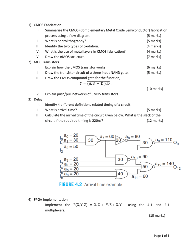
1) CMOS Fabrication I. Summarize the CMOS (Complementary Metal Oxide Semiconductor) fabrication process using a flow diagram. (5 marks) II. What is photolithography? (5 marks) III. Identify the two types of oxidation. (4 marks) IV. What is the use of metal layers in CMOS fabrication? (4 marks) V. Draw the nMOS structure. (7 marks) 2) MOS Transistors I. Explain how the pMOS transistor works. (6 marks) II. Draw the transistor circuit of a three input NAND gate. (5 marks) III. Draw the CMOS compound gate for the function, 𝑌 = ̅̅̅̅̅̅̅̅̅̅̅̅̅̅̅̅̅̅ (A. B + D ). D . (10 marks) IV. Explain push/pull networks of CMOS transistors. 3) Delay I. Identify 4 different definitions related timing of a circuit. II. What is arrival time? (5 marks) III. Calculate the arrival time of the circuit given below. What is the slack of the circuit if the required timing is 220ns? (12 marks) 4) FPGA Implementation I. Implement the F(X, Y, Z) = X. Z + Y. Z + X. Y multiplexers. using the 4-1 and 2-1 (10 marks) Page 1 of 3 II. Design a simple remote controller key pattern generator system with the following specifications. Only the key pattern part is handled in the design. There are three buttons on the controller. When the first one is pressed, the combinational circuit should produce pattern 001 . For the second and third buttons, this pattern will become 010 and 100 , respectively. When more than one button is pressed, the output of the combinational circuit will be the pattern 000 . This pattern will also be used when no button is pressed. Derive the truth table and a Boolean equation for this task. (15 marks) Page 2 of 3 Page 3 of 3
