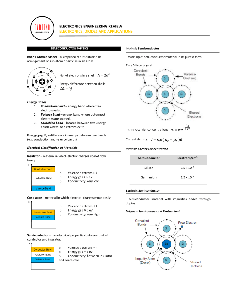
ELECTRONICS ENGINEERING REVIEW ELECTRONICS: DIODES AND APPLICATIONS SEMICONDUCTOR PHYSICS Intrinsic Semiconductor Bohr’s Atomic Model – a simplified representation of arrangement of sub-atomic particles in an atom. - made up of semiconductor material in its purest form. Pure Silicon crystal 2 No. of electrons in a shell: N = 2n Energy difference between shells: E = hf Energy Bands 1. Conduction band – energy band where free electrons exist 2. Valence band – energy band where outermost electrons are located. 3. Forbidden band – located between two energy bands where no electrons exist Intrinsic carrier concentration: ni = Ne Energy gap, Eg – difference in energy between two bands (e.g. conduction and valence bands) Current density: J = ni e ( e + h ) E Electrical Classification of Materials Intrinsic Carrier Concentration Insulator – material in which electric charges do not flow freely. o o o Valence electrons > 4 Energy gap > 5 eV Conductivity: very low − Eg 2kT Semiconductor Electrons/cm3 Silicon 1.5 x 10¹⁰ Germanium 2.5 x 10¹³ Extrinsic Semiconductor Conductor – material in which electrical charges move easily. o o o Valence electrons < 4 Energy gap ≈ 0 eV Conductivity: very high Semiconductor – has electrical properties between that of conductor and insulator. o Valence electrons = 4 o Energy gap ≈ 1 eV o Conductivity: between insulator and conductor - semiconductor material with impurities added through doping. N-type = Semiconductor + Pentavalent Carriers Symbol: Construction: P-type = Semiconductor + Trivalent Biasing • Forward biasing – P connected to positive terminal of source voltage, N to negative terminal. Carriers • Electrical Parameters for Semiconductors Reverse biasing - P connected to negative terminal of source voltage, N to positive terminal. Drift velocity: vd = e E Current: I = neAe E Conductivity: = qn Current density N-type: Jn = e ( nn e + pn h ) E P-type: Jp = e np e + pp h E ( ) Equilibrium condition (Mass Action Law) – the product of the number of electrons in the conduction band and the number of holes in the valence band is constant at a fixed temperature and is independent of amount of donor and acceptor impurity added. ni 2 = np pp SEMICONDUCTOR DIODE - two-terminal device consisting of an N-type and P-type material joined together. Diode Currents Shockley’s Equation for diode forward current kVD ID = IS e T − 1 where k= 11,600 n For low levels of diode current, n = 1 for Ge and n = 2 for Si. For high levels of diode current, n = 1 for both Si and Ge. Temperature effects: Reverse Current: IS1 T −T /10 = IS 0 2( 1 0 ) VTh1 = VTh0 + k (T1 − T0 ) Threshold voltage: Where: k = −2.5mV / oC for Ge Q-factor: Q = 0.159 fRsCt Max power dissipation: PZ max = 4IZT VZ BASIC ZENER CIRCUITS Fixed Vi and RL k = −2.0mV / oC for Si Diode Models and Characteristics 1. Ideal Diode Model – diode acts as switch. 2. Simplified Diode Model – threshold voltage considered Load voltage: V = RLVi = V L Z R + RL Zener current: IZ = IR − IL Power dissipation: PZ = I Z VZ Fixed Vi , variable RL 3. Linear Diode Model – internal resistance and threshold voltage considered (for exact calculations) RVZ Min load resistance: R Lmin = Vi − VZ Diode Resistances • DC Resistance: R = VD D ID • Dynamic resistance: r = 26mV d ID • VD Ave resistance: r ave = ID VZ Max load current: I Lmax = RLmin Min load current: ILmin = IR − IZM VZ Max load resistance: R Lmax = ILmin Variable Vi , fixed RL Power Dissipation: PDmax = IDVD Reverse-recovery time – time needed for current to change direction when diode is switched from forward to reverse conditions. trr = tr + t s SPECIAL PURPOSE DIODES Zener - diode used as a voltage reference. Symbol: Temperature coefficient: TC = VZ VZ (T1 − T0 ) Min input voltage: Vi min = ( R + RL )VZ RL Max series current: IR max = IZM + IL Max input voltage: Vi max = IR max R + VZ Point contact diode Very high capacitance Schottky diode Metal-conductor rectifier Tunnel diode Negative resistance Gunn diode Wideband diode PIN diode Offers impedance at microwave LED Emits light Photodiode Current varies with light Thyrector Bidirectional trigger device Light Emitting Diode (LED) - diode which emits light when forward biased. Light wavelength: = c f Energy: Eg = hc LED Color Construction: Negative resistance – current decreases as voltage increases across the device (opposite of Ohm’s Law). Gunn effect – production of rapid fluctuations of current when the voltage applied to a semiconductor device exceeds a critical value with the result that microwave power is generated. DIODE APPLICATIONS Rectification – process of converting AC to pulsating DC. Important quantities: Varactor Ripple factor: r = Vr (rms) Vdc - diode with variable capacitance. Ripple voltage: Vr (rms) = Vrms2 − Vdc 2 Capacitance: CT = where Half-wave Rectifier k (VT + VR )n 1 for alloy junction 2 1 n = for diffused junction 3 n= In terms of np bias capacitance: C = T Temperature Coefficient: TC = C (0) (1 + VR / VT ) n C C0 (T1 − T0 ) Special Purpose Diodes Diode Characteristics Varactor Variable capacitance Average value: Ideal: Vdc = 0.318Vm Practical: Vdc = 0.318 (Vm − Vth ) Peak Inverse Voltage: PIV = Vm Output frequency: fout = fin Full-wave Rectifier Clipper - circuit which clips a portion of the input signal. Positive Clipper Bridge type Negative Clipper Average value: Ideal: Vdc = 0.636Vm Practical: Vdc = 0.636 (Vm − 2Vth ) Clamper - shifts the input signal to a different dc signal. Peak Inverse Voltage: PIV = Vm Output frequency: fout = 2 fin Center-tapped Note: The peak-to-peak values for the input and output signals are equal. Voltage Multiplier - a circuit which gives an output that is an integral multiple of the input. Voltage Doubler Voltage Tripler Average value: Ideal: Vdc = 0.636Vm Practical: Vdc = 0.636 (Vm − Vth ) Peak Inverse Voltage: PIV = 2Vm Output frequency: fout = 2 fin Review Questions 1. 2. 3. A diode (P-N junction) has two terminals. The P-terminal is known as A. Anode* B. Cathode C. Either anode or cathode D. None of these 9. A working diode must have A. High resistance when forward or reverse biased B. Low resistance when forward biased, while high resistance when reverse bias* C. High resistance when forward biased, while low resistance when reverse bias D. Low resistance when forward or reverse biased 10. When a junction diode is Forward Biased the thickness of the depletion region is A. Larger C. Smaller* B. Medium D. None of these Electrons in p-type material of a semiconductor are called as A. either minority carriers or majority carriers B. minority carriers* C. majority carriers D. valance carriers 4. A diode (p-n junction) when reverse biased act as A. On Switch C. Zener diode B. Capacitor D. Off Switch* 5. Depletion region of a p-n junction is formed A. During Reverse bias B. During Forward bias C. During Manufacturing* D. During Heating 6. 7. 8. A zener diode voltage regulator has load requirement of 12 V and 2 Amp. The zener diode's minimum current requirement is 0.2 A. The minimum voltage at input is 24 V. What is maximum efficiency of circuit? A. 34.3 % C. 45.5 %* B. 52.8 % D. 66.3 % A 3 - phase diode bridge rectifier is fed from a 400 V rms, 50 Hz, 3 phase AC source. If the load is purely resistive, then peak instantaneous output voltage is equal to A. 400√2 V* C. 400 V B. 400√(2/3) V D. 400 / √3 V A LED produces light when A. forward biased* C. reverse biased B. unbiased D. none of these A Schottky diode is a A. majority carrier device* B. minority carrier device C. fast recovery diode D. both a majority and a minority carrier diode 11. If temperature increases then conductivity of a semiconductor is A. Decreases C. Increases* B. Constant D. None of these 12. A semiconductor has a A. Negative Temperature coefficient of resistance* B. Positive Temperature coefficient of resistance C. Constant Temperature coefficient of resistance D. None of the above 13. The leakage current in a pn junction is in order of A. A C. kA B. µA* D. None of these 14. N-type extrinsic semiconductor is obtained by adding A. trivalent impurity B. pentavalent impurity* C. tetravalent impurity D. all of the above 15. The amount of time between the creation and disappearance of a free electrons is called A. recombination B. bound electrons C. drift velocity D. life time of the carriers* 16. Single phase, 230 V, 1 KW heater is connected across single phase 230 V, 50 Hz supply through a diode. The power delivered to the heater element A. 100 W C. 1000 W B. 500 W* D. None of above 17. For a diode, reverse recovery time is defined as the time between the instant diode current becomes zero and the instant reverse recovery current decays to A. 0 B. 10% of reverse peak current C. 25% of reverse peak current* D. 15% of reverse peak current 18. When the pn junction is forward biased the sequence of events that take place are A. diffusion, drift and recombination B. injection, diffusion and recombination* C. diffusion, injection and drift D. none of above 19. The depletion region of a pn junction is one, that is depleted of A. atoms B. mobiles charges* C. immobile charges D. velocity of the carriers 20. The junction capacitance of linearly graded junction varies with the applied reverse bias, VR as A. (VR)- 1 C. (VR)- ½ B. (VR)- 1/3* D. (VR)1/2 21. The diffusion capacitance of a forward biased P+N junction diode with a steady electric current I depends on A. width of the depleted region B. mean life time of the holes C. mean life time of the electrons* D. junction area 22. Avalanche breakdown in a diode occurs when A. potential barrier is reduced to zero B. forward electric current exceeds certain value C. reverse bias exceeds a certain value* D. none of the above 23. Which are the mobile charge carriers present in semiconductor diode? A. Holes C. Neutrons B. Electrons D. Both A & B* 24. If the series resistance increases in an unloaded zener regulator, the zener current A. decreases* B. stays the same C. increases D. equals the voltage divided by the resistance 25. The load voltage is approximately constant when a zener diode is A. forward biased B. reverse biased C. operating in breakdown region* D. unbiased 26. When the source voltage increases in a zener regulator, which of these electric current remain approximately constant? A. Series current C. Zener current B. Load current* D. None of these 27. A silicon material has an intrinsic concentration ni=1010 per cubic centimeter at room temperature. If it is doped with 1015 antimony atoms per cubic centimeter, what is now the approximate electron concentration at the conduction band? A. 105 electrons C. 1010 electrons B. 1015 electrons* D. 1020 electrons B. decrease C. decrease exponentially D. increase* 34. As the operating temperature of a reverse-biased diode is increased, its leakage or reverse saturation current will A. Increase B. increase exponentially* C. decrease D. decrease exponentially 35. For a silicon diode, calculate the current at room temperature if the forward voltage VF = 0.3 V and the reverse saturation current IS = 100 nA. A. 32.8 μA* C. 10.8 μA B. 32.8 mA D. 10.8 mA 28. An external voltage applied to a junction reduces its barrier and aid current to flow through the junction A. reverse bias C. external bias B. junction bias D. forward bias* 36. Calculate the new threshold voltage of a germanium diode when it operates at 100 0C. A. 0.113 V* C. 0.188 V B. 0.215 V D. 0.513 V 29. A device containing an anode and a cathode or a pn junction of a semiconductor as the principal elements and provides unidirectional conduction. A. diode* C. diac B. triode D. triac 37. A silicon diode has a reverse saturation current of 50 nA at room temperature. If the operating temperature is raised by 50°C, what is now the reverse saturation current? A. 105.56 nA C. 287.73 nA B. 827.89 nA D. 1.66 µA* 30. What do you call the very small amount of current that will flow in the diode when it is reverse biased? A. saturation current B. reverse saturation current* C. cut-off current D. holding current 38. In every increase of 10°C in the operating temperature of a diode will cause its reverse saturation current to A. decrease C. double* B. triple D. quadruple 31. The minimum voltage required before a diode can totally conduct in a forward direction. A. triggering voltage B. breakdown voltage C. saturation voltage D. threshold voltage* 32. What will happen to the threshold voltage of the diode when it operates at higher temperatures? A. increases B. increases exponentially C. decreases* D. decreases exponentially 33. The forward current in a conducting diode will _____ as the operating temperature increases. A. not be affected 39. When a diode is reverse biased the depletion region widens, since it is in between positively charge holes and negatively charge electrons, it will have an effect of a capacitor, this capacitance is called what? A. diffusion capacitance B. storage capacitance C. stray capacitance D. transition capacitance* 40. A diode that is especially designed to operate as a voltage-variable capacitor. It utilizes the junction capacitance of a semiconductor diode. A. varactor C. varicap B. varistor D. A and C * 41. The capacitance of a varactor will _______ when the forward bias voltage is increased. A. increase* B. decrease C. exponentially decrease D. not change 42. In operating a diode at high-speed switching circuits, one of the most important parameters to be considered is A. ac resistance B. diode capacitance C. noise figure D. reverse recovery time* 43. The maximum power the diode can handle. A. maximum derating power B. maximum consumption power C. breakdown power D. maximum dissipation power* 44. What will happen to the power handling capability of the diode if it is to be operated at a higher temperature? A. decreases* B. increases C. increases exponentially D. will not be affected 45. A certain diode has a maximum power dissipation of 500 mW at room temperature and a linear power derating factor of 5.0 mW/°C. How much power the diode can handle if operated at 50°C. A. 625 mW C. 505 mW B. 495 mW D. 375 mW* 46. Refers to a special type of diode which is capable of both amplification and oscillation. A. Junction diode B. Tunnel diode* C. Point contact diode D. Zener diode 47. Diode whose negative resistance depends on a specific form of quantum-mechanical bond structure of the material A. Gunn diode* B. tunnel diode C. TRAPATT diode D. backward diode 48. What semiconductor diode that have a fine wire (called a cat-whisker) whose point is in permanent contact with the surface of a wafer of semiconductor material such as silicon, germanium or gallium arsenide? A. point-contact diode* B. diac C. PiN diode D. thyrector 49. The appearance of RF current oscillations in a dc-biased slab of ntype gallium arsenide in a 3.3 kV electric field A. Gunn effect* C. Hall effect B. Zener effect D. avalanche 50. What will happen to the magnitude of the load-line slope when the load resistance is decreased? A. it will also decrease B. it will increase* C. it will increase exponentially D. is not affected by the load 51. A germanium diode is connected to a load resistance of 1.5 kΩ and is supplied with 12-V such that the diode will be forward biased. What is the voltage across the diode? A. approximately 12 V B. approximately 0.7 V C. approximately 0.3 V* D. can’t be solved 52. What is the drop across the diode when it is connected in series to a resistor of 1.8 kΩ and a supply voltage of 50 V? The supply voltage causes the diode to be reversebiased. A. 50 V* C. 0.7 V B. 0.3 V D. can’t be solved 53. Two germanium diodes are connected in series and have a load resistance of 10 kΩ and a forward supply voltage of 5 V. Calculate the voltage across the load resistor. A. 4.7 V C. 4.4 V* B. 0.6 V D. 0.3 V 54. A silicon diode is in parallel with a germanium diode and is connected to a load resistor having a value of 20 kΩ and a forward supply voltage of 10 V. What is the approximate voltage across the silicon diode? A. 10 V C. 1.0 V B. 0.7 V D. 0.3 V* 55. At room temperature, in a perfect silicon crystal, the equilibrium concentration of thermally generated electrons in the conduction band is about A. 1.5 x 10⁵ per cubic cm B. 1.5 x 10¹⁰ per cubic cm* C. 1.5 x 10¹⁵ per cubic cm D. 1.5 x 10²⁰ per cubic cm 56. What is the output voltage across a load resistor if it is paralleled with a forward biased silicon diode? The resistor network is supplied with 10 V. A. 0.7 V* C. 9.3 V B. 10 V D. lack of data 57. How many capacitors are used in a diode-capacitor half- wave voltage doubler? A. 1 C. 2* B. 3 D. 4 58. In a diode-capacitor voltage quadrupler, what is the voltage across the third stage capacitor? A. Vmax C. 2 Vmax* B. 3 Vmax D. 4 Vmax 59. A light emitting diode (LED) is to be used in a circuit with a supply voltage of 5 V. What should be the value of the resistor needed by the LED to operate normally? A. 25 Ω C. 250 Ω* B. 25 kΩ D. 250 kΩ 60. In a semiconductor device, a p-n junction formed by alloying a suitable material such as indium with the semiconductor. A. alloy junction* B. diffused junction C. depletion junction D. storage junction 61. Which of the following is not a valid form of a diode equivalent circuit? A. Piecewise Linear Model B. Ideal Diode Model C. Simplified Model D. Differential Model* 62. Which model of the diode equivalent circuit is represented by the given diagram? A. Piecewise Linear Model* B. Ideal Diode Model C. Simplified Model D. Differential Model 63. AC resistance of a diode was found to be r1 and r2, when measured with two different values of diode current i.e. 10 mA and 25 mA respectively, for the same diode voltage. Which of the following options hold true? A. r1 = r2 B. r1 > r2* C. r1 < r2 D. Can’t be determined 64. The reverse saturation current for a Germanium diode at a temperature of 293 K is found to be 2 μA. What is the reverse saturation current Is at a temperature of 313 K? A. 2 μA B. 8 μA* C. 4 μA D. Can’t be determined 65. The maximum load current that can be drawn is A. 1.4 mA* B. 1.8 mA C. 2.3 mA D. 2.5 mA 66. For the circuit shown diode cutting voltage is Vin = 0. The ripple voltage is to be no more than vrip = 4 V. The minimum load resistance, that can be connected to the output is (in kilo ohm) A. 6.25* B. 25 C. 12.5 D. 30 67. An ideal diode has ____ & _____ A. some forward voltage drop, some reverse recovery time B. high switching losses, high reverse voltage drop C. no forward voltage drop, negligible reverse recovery time* D. no reverse recovery time, high leakage current 68. The figure below shows a circuit for charging a 12-V battery. If Vs is a sinusoid with 24-V peak amplitude, the fraction of each cycle during which the diode conducts is A. One quarter of a cycle B. One-third of a cycle* C. One half of the cycle D. Three quarters of a cycle 69. Diodes can be used in the making of A. Rectifiers B. LED lamps C. Logic gates D. All of the mentioned* 70. For the connections shown below, the equivalent logic gate is A. OR gate* B. XOR gate C. AND gate D. NAND gate 71. For the connections shown below, the equivalent logic gate is 73. A zener diode works on the principle of_________ A. tunneling of charge carriers across the junction* B. thermionic emission C. diffusion of charge carriers across the junction D. hopping of charge carriers across the junction 74. When the voltage across the zener diode increases_________ A. temperature remains constant and crystal ions vibrate with large amplitudes B. temperature increases and crystal ions vibrate with large amplitudes* C. temperature remains constant and crystal ions vibrate with smaller amplitudes D. temperature decreases and crystal ions vibrate with large amplitudes 75. Avalanche breakdown in zener diode is ______ A. electric current multiplication takes place* B. phenomenon of voltage multiplication takes place C. electrons are decelerated for a period of time D. sudden rise in voltage takes place 76. If the positive terminal of the battery is connected to the anode of the diode, then it is known as A. Forward biased* B. Reverse biased C. Equilibrium D. Schottky barrier 77. Ideally the voltage drop across a conducting diode must be A. ∞ B. 0* C. higher than the forward biased voltage D. equal to the forward biased voltage A. OR gate B. XOR gate C. AND gate* D. NAND gate 72. The units frequently used to measure the forward bias and reverse bias current of a diode are A. µA and µA respectively B. µA and mA respectively C. mA and µA respectively* D. mA and mA respectively 78. Schottky diodes are also called as A. metal diode B. hot carrier diode* C. signaling diode D. easy turn on diode 79. In a Schottky diode, the aluminum metal acts as a __________ A. anode* C. cathode B. gate D. none of these 80. Zener diodes allow a current to flow in the reverse direction, when the A. voltage reaches above a certain value* B. temperature reaches above a certain value C. current always flows in the reverse direction only D. current cannot flow in the reverse direction 81. Which of the following equipment can’t be used to check the condition of a diode? A. Digital Display Meter B. Ohmmeter C. Curve Tracer D. CRO* 82. What is the expected reading obtained on a Digital Display Meter with diode-checking function when a proper functioning silicon semiconductor diode is connected across its leads in the forward bias configuration? A. 0.67 V* B. 0.3 V C. Open Loop Indication D. Varies with the diode 83. Even after the forward current reduces to zero value, a practical diode continues to conduct in the reverse direction for a while due to the A. resistance of the diode B. high junction temperature C. stored charges in the depletion region* D. none of the mentioned 84. For a p-n junction diode, the peak inverse current & the reverse recovery time are dependent on A. inverse voltage B. forward Voltage C. di/dt* D. all of the above mentioned 85. In an AC-DC converter, a diode might be used as a A. voltage source B. phase angle controller C. freewheeling Diode* D. filter
