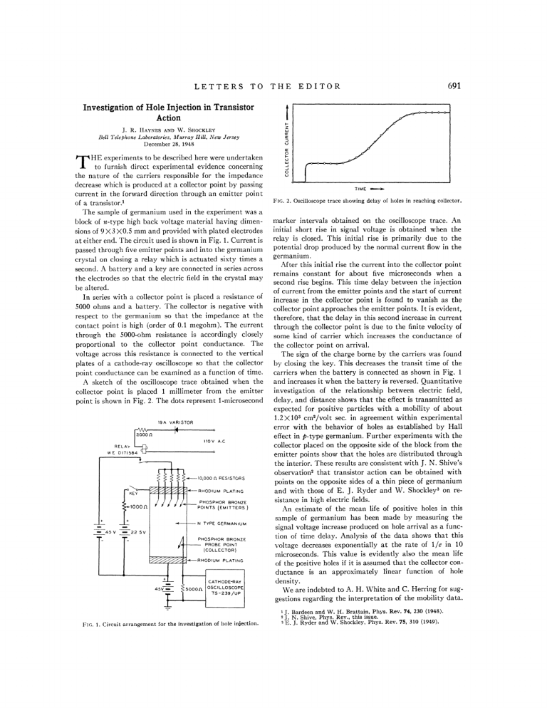
LETTERS TO THE EDITOR 691 Investigation of Hole Injection in Transistor Action J. R. HAYNES AND W. SHOCKLEY Bell Telephone Laboratories, Murray Hill, New Jersey December 28, 1948 T H E experiments to be described here were undertaken to furnish direct experimental evidence concerning the nature of the carriers responsible for the impedance decrease which is produced at a collector point by passing current in the forward direction through an emitter point of a transistor. 1 The sample of germanium used in the experiment was a block of w-type high back voltage material having dimensions of 9X3X0.5 mm and provided with plated electrodes at either end. The circuit used is shown in Fig. 1. Current is passed through five emitter points and into the germanium crystal on closing a relay which is actuated sixty times a second. A battery and a key are connected in series across the electrodes so that the electric field in the crystal may be altered. In series with a collector point is placed a resistance of 5000 ohms and a battery. The collector is negative with respect to the germanium so that the impedance a t the contact point is high (order of 0.1 megohm). The current through the 5000-ohm resistance is accordingly closely proportional to the collector point conductance. The voltage across this resistance is connected to the vertical plates of a cathode-ray oscilloscope so that the collector point conductance can be examined as a function of time. A sketch of the oscilloscope trace obtained when the collector point is placed 1 millimeter from the emitter point is shown in Fig. 2. The dots represent 1-microsecond 19A VARISTOR 10,000 n RESISTORS RHODIUM PLATING PHOSPHOR BRONZE POINTS (EMITTERS ) N TYPE GERMANIUM PHOSPHOR BRONZE — PROBE POINT (COLLECTOR) -RHODIUM PLATING CATHODE-RAY OSCILLOSCOPE TS-239/UP FIG. 1. Circuit arrangement for the investigation of hole injection. FIG. 2. Oscilloscope trace showing delay of holes in reaching collector. marker intervals obtained on the oscilloscope trace. An initial short rise in signal voltage is obtained when the relay is closed. This initial rise is primarily due to the potential drop produced by the normal current flow in the germanium. After this initial rise the current into the collector point remains constant for about five microseconds when a second rise begins. This time delay between the injection of current from the emitter points and the start of current increase in the collector point is found to vanish as the collector point approaches the emitter points. It is evident, therefore, that the delay in this second increase in current through the collector point is due to the finite velocity of some kind of carrier which increases the conductance of the collector point on arrival. The sign of the charge borne by the carriers was found by closing the key. This decreases the transit time of the carriers when the battery is connected as shown in Fig. 1 and increases it when the battery is reversed. Quantitative investigation of the relationship between electric field, delay, and distance shows that the effect is transmitted as expected for positive particles with a mobility of about 1.2 X10 3 cm 2 /volt sec. in agreement within experimental error with the behavior of holes as established by Hall effect in p-type germanium. Further experiments with the collector placed on the opposite side of the block from the emitter points show that the holes are distributed through the interior. These results are consistent with J. N. Shive's observation 2 that transistor action can be obtained with points on the opposite sides of a thin piece of germanium and with those of E. J. Ryder and W. Shockley 3 on resistance in high electric fields. An estimate of the mean life of positive holes in this sample of germanium has been made by measuring the signal voltage increase produced on hole arrival as a function of time delay. Analysis of the data shows that this voltage decreases exponentially a t the rate of 1/e in 10 microseconds. This value is evidently also the mean life of the positive holes if it is assumed that the collector conductance is an approximately linear function of hole density. We are indebted to A. H. White and C. Herring for suggestions regarding the interpretation of the mobility data. i2 J. Bardeen and W. H. Brattain, Phys. Rev. 74, 230 (1948). J. N. Shive, Phys. Rev., this issue. 3 E. J. Ryder and W. Shockley, Phys. Rev. 75, 310 (1949).


