A Noise and RTN-Removal Smart Method for
the Parameter Extraction of CMOS Aging
Compact Models
Javier Diaz-Fortuny1, Javier Martin-Martinez1, Rosana Rodriguez1, Rafael Castro-Lopez2, Elisenda Roca2,
Francisco F. Fernandez2 and Montserrat Nafria1
1
Universitat Autònoma de Barcelona (UAB), Electronic Engineering Department, REDEC group, Barcelona, Spain
2
Instituto de Microelectrónica de Sevilla, IMSE-CNM, CSIC and Universidad de Sevilla, Spain
email1: {javier.diaz; javier.martin.martinez; rosana.rodriguez; montse.nafria}@uab.es
email2: {castro; eli; francisco.fernandez}@imse-cnm.csic.es.
Abstract— In this work, a new method for the statistical
obtention of the emission times and related ∆Vth of
nanometer CMOS transistors’ oxide defects is presented.
The method identifies the Vth drops associated to oxide
trap emissions during BTI and HCI aging recovery traces
while removing RTN and background noise contributions
to avoid artifacts during data analysis.
Keywords- CMOS; BTI; HCI; parameters; extraction;
method; RTN; defects; aging;
I. INTRODUCTION
With nowadays CMOS technology downscaling, BTI
and HCI aging and RTN transient effects, have
reemerged as important time-dependent variability
(TDV) phenomena that must be taken into account in the
design of digital and analog VLSI integrated circuits
(ICs). During circuit operation, these variability effects,
related to the trapping/detrapping in/from oxide defects,
could result in circuit malfunction due to the shift of
some transistors’ parameters, such as the threshold
voltage (Vth) [1]. Thus, it is critical for IC circuit
designers to take into account TDV effects to implement
reliability-aware circuits [2]. For this, TDV compact
models that distinguish the defects contribution due to
aging from that due to RTN and other noise sources are
necessary. On the other hand, an accurate defects
parameters extraction method requires statistical
characterization of transistors under accelerated
conditions [3].
Conventional
BTI/HCI
aging
characterization
techniques are based in the application of serialized
measurement-stress-measurement sequences to one or a
few CMOS transistors simultaneously by using probe
stations. However, to get sufficient statistical data, a
massive aging test, with hundreds of transistors, must be
performed. Doing so serially (one device at a time) may
however take several months. In our work, we use the
65-nm technology ENDURANCE IC chip to execute
BTI/HCI aging tests over hundreds of CMOS transistors
with a stress parallelization technique that significantly
reduces the total aging test time [4]. Aging can be
modeled by analyzing the emission times (τe) and related
∆Vth (η) of defects during the recovery phases after the
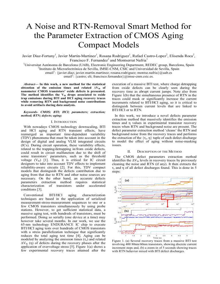
application of overvoltage stress [5]. Figure 1(a) shows a
few experimental recovery traces attained after the
execution of a massive BTI test, where charge detrapping
from oxide defects can be clearly seen during the
recovery time as abrupt current jumps. Note also from
Figure 1(b) that the simultaneous presence of RTN in the
traces could mask or significantly increase the current
increments related to BTI/HCI aging, so it is critical to
distinguish between current levels that are linked to
BTI/HCI or to RTN.
In this work, we introduce a novel defects parameter
extraction method that massively identifies the emission
times and η values in experimental transistor recovery
traces when RTN and background noise are present. The
defect parameter extraction method ‘cleans’ the RTN and
background noise from the recovery traces and performs
the extraction of the {τe, η} tuple of each defect discharge
to model the effect of aging without noise-masking
issues.
II.
DESCRIPTION OF THE METHOD
The CMOS defect parameters extraction method
identifies the ∆Vth levels in recovery traces by previously
cleaning the noise and RTN (if any). It then extracts the
τe and η of all defect discharges found. This is done in 5
steps:
Figure 1. (a) Several recovery traces from a massive BTI test
involving 400 80nm/60nm transistors, showing discrete current
increment steps and, (b) a zoom-in of 5 seconds showing traces
with RTN behavior mixed with BTI defect discharges.
1) For each tested device, the IDS measured as a
function of time during the measurement phase of the
aging test is converted into the equivalent ∆Vth by means
of the pre-stressed IDS-VGS curve [6].
2) The next step consists in the application of the
Weighted Time Lag Method (WTLM) to the full
recovery trace, in order to identify the number and value
of ∆Vth levels present [7].
3) Once the ∆Vth levels are identified, the method
filters out the background noise of the trace and assigns,
to each sample in the ∆Vth trace, the closest ∆Vth level
obtained with the WTLM. This step digitizes the ∆Vth
recovery trace, erasing the backgroud noise and leaving
only ∆Vth levels associated to BTI/HCI discharges and
RTN phenomena. For instance, Figure 2 (a) shows two
∆Vth traces (blue traces), both showing high ∆Vth
degradation due to previous stress, and also displays the
∆Vth trace reconstruction (red trace) with the
background noise removed. During the recovery period
(i.e., from 2ms to 100s), different Vth levels can be
observed because of defect emissions mixed with RTN
phenomena, as shown in the zooms in Figure 2(b) and
(c).
4) In order to distiguish between RTN and BTI/HCI
emissions, the method registers and stores the transitions
between different ∆Vth levels. In the case of RTN, fast
defects identification leads to multiple transitions
between two ∆Vth levels while, for slow defects
emissions, only a single transistion between two ∆Vth
levels is counted.
5) The last step consists in obtaining τe and η
parameters of only the aging related discharges, using the
information in step 4, that can be easily evaluated from
the filtered ∆Vth trace, as shown in Figure 2(d). For this
example, a total of 4 and 3 discharges are extracted from
trace 1 and trace 2, respectively.
III.
METHOD APPLICATION
In order to evaluate the parameter extraction method, 4
BTI tests, each one involving 138 CMOS transistors with
8 different channel sizes (i.e., W and L), will be
considered for defect extraction. The accelerated stress
consisted in 4 stress/measurement cycles with increasing
VGS stress at 1.2V, 1.5V, 2V and 2.5V and VDS at 0V,
while measurement (i.e., recovery) phases were set at
VGS ≈ Vth and VDS = 0.1V. The parameters extracted
from the BTI tests using the proposed method have
identified a total of 2,625 aging defect emissions, as
shown in Figure 3(a).
The figure verifies that by increasing the stress voltage
(i.e., VGS ≥ 1.2V) a large number of defects are detected
because defects with smaller capture times are activated.
Figure 3(b) shows the exponential distribution of η for
the 8 different geometries, showing that <η> increases as
the area of the tested devices decreases. If the RTN
phenomena was not removed from the recovery traces
before the slow defects identification, a large number of
‘false’ defects (with equal ∆Vth value as the RTN
amplitude) would have been taken into account during
the <η> calculation. Therefore, the resulting <η> value
would have been close to the ∆Vth of the fastest RTN,
masking the actual <η> of the defects.
Figure 3. (a) Distribution of number of defects as a function
of τe for each gate stress voltage. (b) Cumulative distribution
function of the η values extracted from a 4 cycle BTI test with
VGS = 2.5V and different W/L ratios.
ACKNOWLEDGMENT
This work has been supported in part by the TEC201345638-C3-R and TEC2016-75151-C3-R Projects (funded
by the Spanish MINECO and ERDF) and by the P12TIC-1481 Project (funded by Junta de Andalucía).
REFERENCES
Figure 2. (a) Recovery traces from two different devices
(blue) with the reconstructed trace without noise (red). (b), (c)
Zoom in the signals showing RTN (blue traces) and trace
reconstruction without background noise (red traces). (d)
Filtered recovery traces without noise and RTN ready for
defect parameter extraction.
[1]
[2]
[3]
[4]
[5]
[6]
[7]
B. Kaczer et al., IRPS (2010), pp. 26–32.
A. Toro-Frias et al., VLSI J., vol. 55, no. 1, pp. 341–348, 2016.
J. Martin-Martinez et al., IRPS (2011), pp. 920–925.
J. Diaz-Fortuny et al., SMACD (2017), pp. 1–4.
T. Grasser et al., IRPS (2010), pp. 16–25.
B. Kaczer et al., IRPS (2008), pp. 20-27.
J. Martin-Martinez et al., EDL, vol. 35, no. 4, pp. 479–481, 2014.
