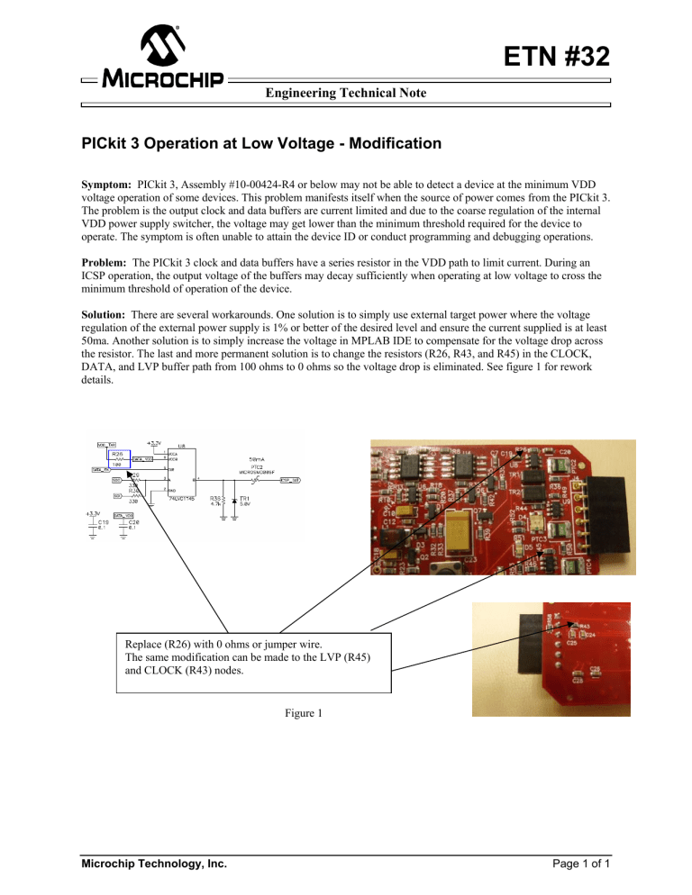
ETN #32 Engineering Technical Note PICkit 3 Operation at Low Voltage - Modification Symptom: PICkit 3, Assembly #10-00424-R4 or below may not be able to detect a device at the minimum VDD voltage operation of some devices. This problem manifests itself when the source of power comes from the PICkit 3. The problem is the output clock and data buffers are current limited and due to the coarse regulation of the internal VDD power supply switcher, the voltage may get lower than the minimum threshold required for the device to operate. The symptom is often unable to attain the device ID or conduct programming and debugging operations. Problem: The PICkit 3 clock and data buffers have a series resistor in the VDD path to limit current. During an ICSP operation, the output voltage of the buffers may decay sufficiently when operating at low voltage to cross the minimum threshold of operation of the device. Solution: There are several workarounds. One solution is to simply use external target power where the voltage regulation of the external power supply is 1% or better of the desired level and ensure the current supplied is at least 50ma. Another solution is to simply increase the voltage in MPLAB IDE to compensate for the voltage drop across the resistor. The last and more permanent solution is to change the resistors (R26, R43, and R45) in the CLOCK, DATA, and LVP buffer path from 100 ohms to 0 ohms so the voltage drop is eliminated. See figure 1 for rework details. Replace (R26) with 0 ohms or jumper wire. The same modification can be made to the LVP (R45) and CLOCK (R43) nodes. Figure 1 Microchip Technology, Inc. Page 1 of 1


