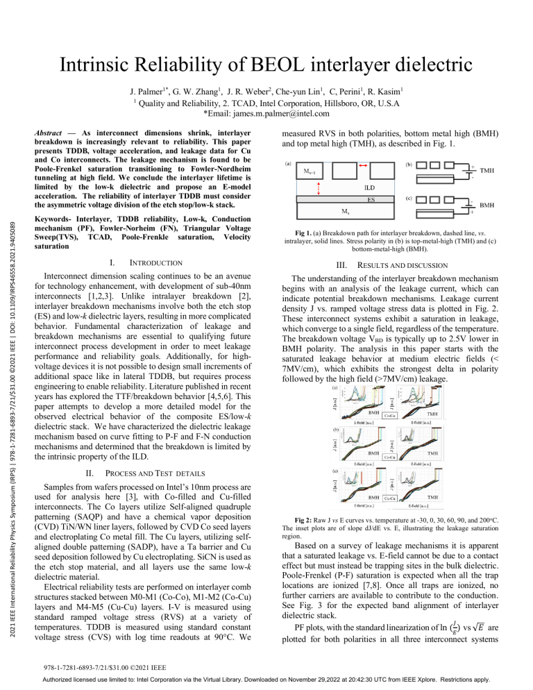
Intrinsic Reliability of BEOL interlayer dielectric J. Palmer1*, G. W. Zhang1, J. R. Weber2, Che-yun Lin1, C, Perini1, R. Kasim1 1 Quality and Reliability, 2. TCAD, Intel Corporation, Hillsboro, OR, U.S.A *Email: james.m.palmer@intel.com 2021 IEEE International Reliability Physics Symposium (IRPS) | 978-1-7281-6893-7/21/$31.00 ©2021 IEEE | DOI: 10.1109/IRPS46558.2021.9405089 Abstract — As interconnect dimensions shrink, interlayer breakdown is increasingly relevant to reliability. This paper presents TDDB, voltage acceleration, and leakage data for Cu and Co interconnects. The leakage mechanism is found to be Poole-Frenkel saturation transitioning to Fowler-Nordheim tunneling at high field. We conclude the interlayer lifetime is limited by the low-k dielectric and propose an E-model acceleration. The reliability of interlayer TDDB must consider the asymmetric voltage division of the etch stop/low-k stack. Keywords- Interlayer, TDDB reliability, Low-k, Conduction mechanism (PF), Fowler-Norheim (FN), Triangular Voltage Sweep(TVS), TCAD, Poole-Frenkle saturation, Velocity saturation I. INTRODUCTION Interconnect dimension scaling continues to be an avenue for technology enhancement, with development of sub-40nm interconnects [1,2,3]. Unlike intralayer breakdown [2], interlayer breakdown mechanisms involve both the etch stop (ES) and low-k dielectric layers, resulting in more complicated behavior. Fundamental characterization of leakage and breakdown mechanisms are essential to qualifying future interconnect process development in order to meet leakage performance and reliability goals. Additionally, for highvoltage devices it is not possible to design small increments of additional space like in lateral TDDB, but requires process engineering to enable reliability. Literature published in recent years has explored the TTF/breakdown behavior [4,5,6]. This paper attempts to develop a more detailed model for the observed electrical behavior of the composite ES/low-k dielectric stack. We have characterized the dielectric leakage mechanism based on curve fitting to P-F and F-N conduction mechanisms and determined that the breakdown is limited by the intrinsic property of the ILD. II. PROCESS AND TEST measured RVS in both polarities, bottom metal high (BMH) and top metal high (TMH), as described in Fig. 1. Fig 1. (a) Breakdown path for interlayer breakdown, dashed line, vs. intralayer, solid lines. Stress polarity in (b) is top-metal-high (TMH) and (c) bottom-metal-high (BMH). III. RESULTS AND DISCUSSION The understanding of the interlayer breakdown mechanism begins with an analysis of the leakage current, which can indicate potential breakdown mechanisms. Leakage current density J vs. ramped voltage stress data is plotted in Fig. 2. These interconnect systems exhibit a saturation in leakage, which converge to a single field, regardless of the temperature. The breakdown voltage VBD is typically up to 2.5V lower in BMH polarity. The analysis in this paper starts with the saturated leakage behavior at medium electric fields (< 7MV/cm), which exhibits the strongest delta in polarity followed by the high field (>7MV/cm) leakage. DETAILS Samples from wafers processed on Intel’s 10nm process are used for analysis here [3], with Co-filled and Cu-filled interconnects. The Co layers utilize Self-aligned quadruple patterning (SAQP) and have a chemical vapor deposition (CVD) TiN/WN liner layers, followed by CVD Co seed layers and electroplating Co metal fill. The Cu layers, utilizing selfaligned double patterning (SADP), have a Ta barrier and Cu seed deposition followed by Cu electroplating. SiCN is used as the etch stop material, and all layers use the same low-k dielectric material. Electrical reliability tests are performed on interlayer comb structures stacked between M0-M1 (Co-Co), M1-M2 (Co-Cu) layers and M4-M5 (Cu-Cu) layers. I-V is measured using standard ramped voltage stress (RVS) at a variety of temperatures. TDDB is measured using standard constant voltage stress (CVS) with log time readouts at 90°C. We Fig 2: Raw J vs E curves vs. temperature at -30, 0, 30, 60, 90, and 200 oC. The inset plots are of slope dJ/dE vs. E, illustrating the leakage saturation region. Based on a survey of leakage mechanisms it is apparent that a saturated leakage vs. E-field cannot be due to a contact effect but must instead be trapping sites in the bulk dielectric. Poole-Frenkel (P-F) saturation is expected when all the trap locations are ionized [7,8]. Once all traps are ionized, no further carriers are available to contribute to the conduction. See Fig. 3 for the expected band alignment of interlayer dielectric stack. 𝐽 PF plots, with the standard linearization of ln(𝐸 ) vs √𝐸 are plotted for both polarities in all three interconnect systems 978-1-7281-6893-7/21/$31.00 ©2021 IEEE Authorized licensed use limited to: Intel Corporation via the Virtual Library. Downloaded on November 29,2022 at 20:42:30 UTC from IEEE Xplore. Restrictions apply. (shown in full paper). All three systems were found to have a P-F slope β of 0.2-0.25. For uncompensated carriers, β is expected to have a factor two [8]. These values are consistent with the dielectric constant of the low-k dielectric common to all three interconnect systems studied in this paper. Fig 5. Leakage current vs. time for (a) Co-Co, (b), Co-Cu, and (c) Cu-Cu. Comparison of intra- and interlayer TTF vs E-field for (d) Co and (e) Cu interconnects. Fig 3 (a) Band alignment for interlayer system. (b) Energy bands in TMH polarity and (c) BMH polarity. The PF trap energy can be extracted from the saturation field 𝐸𝑠 or the thermal activation energy (shown in the full paper). 𝐸𝑠 is read from the slope of ln(𝐽/𝐸) vs √𝐸 vanishing. 𝜑𝐵 is calculated from 𝐸𝑠 = 𝜋𝜖𝜑𝐵 2 /𝑞 [8,9]. We see that Es is between 5-6.5MV/cm in Cu-Cu and 7-8MV/cm for Co-Co, which corresponds to 𝜑𝐵 = 1-1.1eV and 1.1-1.25eV respectively. The Arrhenius thermal activation energy follows 𝜑𝑒𝑓𝑓 = 𝜑0 - β√𝐸 , where 𝜑0 is the trap energy depth and β is the P-F slope. In general, both methods arrive at similar trap energy depths. The trap density is estimated from the saturation current density (100A/µm2). With reference to the electron velocity in SiO2 [9] and 𝐽 = 𝜌𝑣, we derived a density of roughly 5x1020 cm-3. Based on the data, we conclude that the thermochemical Emodel is the best explanation for breakdown.[10] At electric fields >8 MV/cm it is possible that there is some additional degradation due to the tunneling current, but this is not expected to play any role at use condition where P-F saturation occurs. Given the estimated trap density and lack of SILC in contrast to other observations of interlayer TDDB [4], it is questionable whether traps play any role in the breakdown. We believe this rules out a 1/E or √𝐸 based acceleration models and instead propose to follow the thermochemical E-model. IV. CONCLUSIONS Based on the leakage data, the interlayer leakage mechanism is found to be P-F showing carrier density saturation at medium electric fields and F-N tunneling at high electric fields. A P-F trap depth of ~1eV is estimated and the FN barrier height is similarly ~1eV. We conclude that the interlayer lifetime is limited by the low-k dielectric and a thermochemical E-model is proposed for the lifetime acceleration. The reliability assessment of interlayer TDDB must consider the asymmetrical voltage division due to the unequal dielectric constants in the ES/low-k stack. REFERENCES Fig 4. Fit to F-N tunneling form at high field ( >7MV/cm) for (a) Co-Co, (b), Co-Cu, and (c) Cu-Cu. Above 7 MV/cm, by plotting ln(𝐽/𝐸) vs √𝐸, excellent fits to the F-N tunneling form are observed, shown in Fig. 4. The electron effective mass m* is assumed to be 1me [10], although dangling bonds may increase m*. The barrier height does not show consistent polarity dependence, consistent with overlapping I-V curves in Fig. 2 and is 1+/- 0.2 eV high. We believe this strongly suggests a form of tunneling at high electric field. Leakage vs. time for a single field are plotted in Fig. 5. The leakage does not show any stress-induced artifacts (SILC). The voltage acceleration to use condition is reasonable and meets lifetime goals for the expected use conditions. A comparison of intra- to interlayer TTF vs E-field is included in Fig. 5. Interlayer TTF has an acceleration factor comparable to intralayer in both cases, where γ ~ 5cm/MV, and did not show a statistically significant departure from the E-model. [1] R. Chau, “Process and Packaging Innovations for Moore’s Law Continuation and Beyond”, IEDM 2020 [2] G. Zhang et al, “Intrinsic Reliability Study in Low-k Dielectrics with Co Metallurgy in 10nm Process,” IITC, 2020 [3] C. Auth, et al, “A 10nm High Performance and Low-Power CMOS Technology Featureing 3 rd Generation FinFET Transistors, Self-Aligned Quad Pattering, Contact Over Active Gate and Cobalt Local Interconnects,” IEDM, pp. 6E.3-1 -6E3-5, 2018 [4] N. Suzumura et al, “Study on Vertical TDDB Degradation Mechanism and its Relation to Lateral TDDB in Cu/Low-k Damascene Structures”, IRPS, pp 3A4.1-3A4.6, 2014 [5] M. Liang “Polarity Dependence on Electrical Properties of Low-k Dielectric in Copper Interconnect Structures” SSDM 2012 [6] N. Suzumura et al, “Impact of Anode-side Defect Generation on Inter-Level TDDB Degradation in Cu/Low-k Damascene Structures” IRPS, 2020 [7] R. Ongaro, A. Pillonnet. “Poole-Frenkel (PF) effect high field saturation.” Revue de Physique Appliquee, 1989, 24 (12), pp.1085-1095. [8] W.R. Harrell, J. Frey. “Observation of Poole–Frenkel effect saturation in SiO2 and other insulating films”, Thin Solid Films 352 (1999) 195-204 [9] V.A. Gritsenko et al. “Electronic structure of amorphous Si02: Experiment and numerical simulation”, JETP 81 (6), 1995 [10] J. W. McPherson and H.C Mogul “Underlying physics of the thermochemical E model in describing low-field time-dependent dielectric breakdown in SiO2 thin films,” J. Appl. Phys. 84:3, 1513-1523. Authorized licensed use limited to: Intel Corporation via the Virtual Library. Downloaded on November 29,2022 at 20:42:30 UTC from IEEE Xplore. Restrictions apply.


