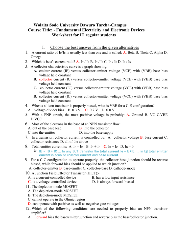
Wolaita Sodo University Dawuro Tarcha-Campus Course Title: - Fundamental Electricity and Electronic Devices Worksheet for IT regular students I. Choose the best answer from the given alternatives 1. A current ratio of IC/IE is usually less than one and is called: A. Beta B. Theta C. Alpha D. Omega 2. Which is beta's current ratio? A. IC / IB B. IC / IE C. IC / IE D. IE / IB 3. A collector characteristic curve is a graph showing: A. emitter current (IE) versus collector-emitter voltage (VCE) with (VBB) base bias voltage held constant B. collector current (IC) versus collector-emitter voltage (VCE) with (VBB) base bias voltage held constant C. collector current (IC) versus collector-emitter voltage (VCE) with (VBB) base bias voltage held constant D. collector current (IC) versus collector-emitter voltage (VCC) with (VBB) base bias voltage held constant 4. When a silicon transistor is properly biased, what is VBE for a C-E configuration? A. voltage-divider bias B. 0.3 V C. 0.7 V D. 0.0 V 5. With a PNP circuit, the most positive voltage is probably: A. Ground B. VC C.VBE D.VCC 6. Most of the electrons in the base of an NPN transistor flow: A. out of the base lead B. into the collector C. into the emitter D. into the base supply 7. In a transistor, collector current is controlled by: A. collector voltage B. base current C. collector resistance D. all of the above 8. Total emitter current is: A. IE – IC B. IC + IE C. IB + IC D. IB – IC IE = IB + IC ... In any BJT transistor the total current Ie = Ic+Ib. ... in bjt total emitter current is equal to collector current and base current. 9. For a C-C configuration to operate properly, the collector-base junction should be reverse biased, while forward bias should be applied to which junction? A. collector-emitter B. base-emitter C. collector-base D. cathode-anode 10. A Junction Field Effector Transistor (JFET):A. is a current-controlled device B. has a low input resistance C. is a voltage-controlled device D. is always forward-biased 11. The depletion-mode MOSFET A. The depletion-mode MOSFET B. The depletion-mode MOSFET C. cannot operate in the Ohmic region D. can operate with positive as well as negative gate voltages 12. Which of the following conditions are needed to properly bias an NPN transistor amplifier? A. Forward bias the base/emitter junction and reverse bias the base/collector junction. B. Forward bias the collector/base junction and reverse bias the emitter/base junction. C. Apply a positive voltage on the n-type material and a negative voltage on the p-type material. D. Apply a large voltage on the base. 13. Junction Field Effect Transistors (JFET) contain how many diodes? A. 4 B. 3 C. 2 D. 1 14. A "U" shaped, opposite-polarity material built near a JFET-channel center is called the: A. Gate B. Block C. Drain D. heat sink 15. In the constant-current region, how will the IDS change in an n-channel JFET? A. As VGS decreases ID decreases. B. As VGS increases ID increases. C. As VGS decreases ID remains constant. D. As VGS increases ID remains constant. 16. A MOSFET has how many terminals? A. 2 or 3 B. 3 C. 4 D. 3 or 4 17. IDSS can be defined as: A. the minimum possible drain current B. the maximum possible current with VGS held at –4 V C. the maximum possible current with VGS held at 0 V D. the maximum drain current with the source shorted 18. What is the input impedance of a common-gate configured JFET? A. very low B. low C. high D. very high 19. JFET terminal "legs" are connections to the drain, the gate, and the: A. Channel B. Source C. Substrate D. Cathode 20. With the E-MOSFET, when gate input voltage is zero, drain current is: A. at saturation B. zero C. IDSS D. widening the channel 21. Which JFET configuration would connect a high-resistance signal source to a low resistance load? A. source follower B. common-source C. common-drain D. common-gate 22.How will electrons flow through a p-channel JFET? A. from source to drain B. from source to gate C. from drain to gate D. from drain to source 23. When VGS = 0 V, a JFET is: A. Saturated B. an analog device C. an open switch D. cut off 24. When applied input voltage varies the resistance of a channel, the result is called: A. Saturation B. Polarization C. Cutoff D. field effect 25. When the JFET is no longer able to control the current, this point is called the: A. breakdown region B. depletion region C. saturation point D. pinch-off region 26.With a JFET, a ratio of output current change against an input voltage change is called: A. Trans conductance B. Siemens C. Resistivity D. Gain 27.The trans conductance curve of a JFET is a graph of: A. IS versus VDS B. IC versus VCE C. ID versus VGS D. ID × RDS 28.The common-source JFET amplifier has: A. a very high input impedance and a relatively low voltage gain B. a high input impedance and a very high voltage gain C. a high input impedance and a voltage gain less than 1 D. no voltage gain 29. Which component is considered to be an "OFF" device? A. Transistor B. JFET C. D-MOSFET D. E-MOSFET 30. In an n-channel JFET, what will happen at the pinch-off voltage? A. the value of VDS at which further increases in VDS will cause no further increase in ID B. the value of VGS at which further decreases in VGS will cause no further increases in ID C. the value of VDG at which further decreases in VDG will cause no further increases in ID D. the value of VDS at which further increases in VGS will cause no further increases in ID 31.In a common emitter transistor amplifier, the output resistance is 500 KΩ and the current gain β = 49. If the power gain of the amplifier is 5×10⁶, the input resistance is :- A. 325 Ω B. 165 Ω C. 225 Ω D. 240 Ω 32. The current gain of a transistor in common base mode is 0.995. The current gain of the same transistor in common emitter mode is A. 197 B. 201 C. 198 D. 199 33.A transistor amplifier circuit is operated with an emitter current of 2 mA. The collector current is 1.98 mA. The common emitter current gain (βdc) of the transistor used in the circuit is:- A. 50 B. 100 C. 125 D. 200 34.In an NPN transistor 108 electrons enter the emitter in 10–8 s. If 1% electrons are lost in the base, the fraction of current that enters the collector and current amplification are respectively A. 0.8 and 49 B. 0.9 and 90 C. 0.7 and 50 D. 0.99 and 99 35. In an NPN power transistor, the collector current is 20 mA. If 98% of the electrons injected in to the base region reach the collector, the base current in mA is nearly A. 2 mA B. 1 mA C. 0.5 mA D. 0.4 mA 36.The current gain α of a transistor is 0.995. If the change in emitter current is 10 mA, the change in base current is A. 50 μA B. 100 μA C. 500 μA D. 25 μA 37. If α and β are the current gains in the CB and CE configurations respectively of the transistor circuit, then (β – α)/αβ is equal to: A. ∞ B. 1 C. 2 D. 0.5 38.A transistor has a βDC of 250 and a base current, IB, of 20 µA. The collector current, IC, equals: A. 500 A B. 5 mA C. 50 mA D. 5 A 39. If an input signal ranges from 20–40 µA (micro amps), with an output signal ranging from 5–1.5 mA (milliamps), what is the ac beta? A. 0.05 B. 20 C. 50 D. 500 40. What is the current gain for a common-base configuration where IE = 4.2 mA and IC = 4.0 mA? A. 16.80 B. 1.05 C. 0.20 D. 0.95 41. What is the collector current for a CE configuration with a beta of 100 and a base current of 30 µA? A. 30µA B. 0.3 µA C. 3 mA D. 3 MA 42.If the common emitter current gain βdc of the transistor used in the amplifier circuit is 200 and the quiescent emitter current is 1 mA, the quiescent base current of the transistor is very nearly equal to: A. 1 mA B. 1 μA C. 2 μA D. 5 μA 43. The collector supply voltage is 6 V and the voltage drop across a resistor of 600 Ω in the collector circuit is 0.6 V, in a transistor connected in common emitter mode. If the current gain is 20, the base current is: A. 0.25 Ma B. 0.05 mA C. 0.02 mA D. 0.07 mA 44.In CB Configuration of transistor, the input impedance is: A. High B. Medium C. Low D. none of these 45. BJT is ———–device. A. Bipolar B. Unipolar C. Constant current D. Constant voltage 46.Transistor is used as: A. Switch B. Amplifier C. Both (a) & (b) D. None of these 47. For a common emitter circuit if IC /IE = 0.98 then current gain for common emitter circuit will be: A.49 B. 98 C. 4.9 D. 25.5 48. When an NPN transistor is used as an amplifier then? A. the electrons flow from emitter to collector B. the holes flow from emitter to collector C. the electrons flow from collector to emitter D. the electrons flow from battery to emitter 49. The current gain for a transistor working as common-base amplifier is 0.96. If the emitter current is 7.2 mA, then the base current is: A. 0.29mA B. 0.35mA C. 0.39 mA D. 0.43 mA 50. In a common base amplifier the phase difference between the input signal voltage and the output voltage is? A. 0 B. π / 4 C. π / 2 D. π


