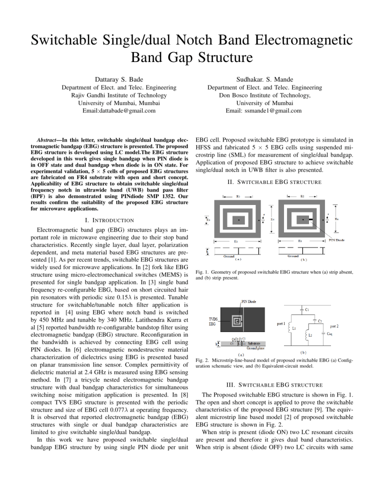
Switchable Single/dual Notch Band Electromagnetic Band Gap Structure Dattaray S. Bade Sudhakar. S. Mande Department of Elect. and Telec. Engineering Rajiv Gandhi Institute of Technology University of Mumbai, Mumbai Email:dattabade@gmail.com Department of Elect. and Telec. Engineering Don Bosco Institute of Technology, University of Mumbai Email: ssmande1@gmail.com Abstract—In this letter, switchable single/dual bandgap electromagnetic bandgap (EBG) structure is presented. The proposed EBG structure is developed using LC model.The EBG structure developed in this work gives single bandgap when PIN diode is in OFF state and dual bandgap when diode is in ON state. For experimental validation, 5 × 5 cells of proposed EBG structures are fabricated on FR4 substrate with open and short concept. Applicability of EBG structure to obtain switchable single/dual frequency notch in ultrawide band (UWB) band pass filter (BPF) is also demonstrated using PINdiode SMP 1352. Our results confirm the suitability of the proposed EBG structure for microwave applications. EBG cell. Proposed switchable EBG prototype is simulated in HFSS and fabricated 5 × 5 EBG cells using suspended microstrip line (SML) for measurement of single/dual bandgap. Application of proposed EBG structure to achieve switchable single/dual notch in UWB filter is also presented. II. S WITCHABLE EBG STRUCTURE I. I NTRODUCTION Electromagnetic band gap (EBG) structures plays an important role in microwave engineering due to their stop band characteristics. Recently single layer, dual layer, polarization dependent, and meta material based EBG structures are presented [1]. As per recent trends, switchable EBG structures are widely used for microwave applications. In [2] fork like EBG structure using micro-electromechanical switches (MEMS) is presented for single bandgap application. In [3] single band frequency re-configurable EBG, based on short circuited hair pin resonators with periodic size 0.15λ is presented. Tunable structure for switchable/tunable notch filter application is reported in [4] using EBG where notch band is switched by 450 MHz and tunable by 340 MHz. Latithendra Kurra et al [5] reported bandwidth re-configurable bandstop filter using electromagnetic bandgap (EBG) structure. Reconfiguration in the bandwidth is achieved by connecting EBG cell using PIN diodes. In [6] electromagnetic nondestructive material characterization of dielectrics using EBG is presented based on planar transmission line sensor. Complex permittivity of dielectric material at 2.4 GHz is measured using EBG sensing method. In [7] a tricycle nested electromagnetic bandgap structure with dual bandgap characteristics for simultaneous switching noise mitigation application is presented. In [8] compact TVS EBG structure is presented with the periodic structure and size of EBG cell 0.077λ at operating frequency. It is observed that reported electromagnetic bandgap (EBG) structures with single or dual bandgap characteristics are limited to give switchable single/dual bandgap. In this work we have proposed switchable single/dual bandgap EBG structure by using single PIN diode per unit Fig. 1. Geometry of proposed switchable EBG structure when (a) strip absent, and (b) strip present. Fig. 2. Microstrip-line-based model of proposed switchable EBG (a) Configuration schematic view, and (b) Equivalent-circuit model. III. S WITCHABLE EBG STRUCTURE The Proposed switchable EBG structure is shown in Fig. 1. The open and short concept is applied to prove the switchable characteristics of the proposed EBG structure [9]. The equivalent microstrip line based model [2] of proposed switchable EBG structure is shown in Fig. 2. When strip is present (diode ON) two LC resonant circuits are present and therefore it gives dual band characteristics. When strip is absent (diode OFF) two LC circuits with same Airline 6 Mode 1 Mode 2 Mode 3 4 2 Frequency (GHz) Frequency (GHz) Airline 6 Mode 1 Mode 2 Mode 3 4 2 Band gap 1.52 GHz - 1.76 GHz 0 50 100 150 0 50 100 150 βd (deg.) βd (deg.) (a) (b) Fig. 3. Dispersion diagram of proposed switchable EBG when ( a ) strip present, and ( b ) strip absent with ( E1 , E2 , E3 , E4 , g, r , h, tan δ) = (7 mm, 5 mm, 1 mm, 3 mm, 2 mm, 4.4, 1.50 mm, 0.02) Epoxy substrate with (r ) = 4.4, substrate height (h) = 1.50 mm. The measurement was conducted with Agilent N9923A network analyzer. The Suspended microstrip line method [2] is used for bandgap measurement. The microstrip line of 50 Ω is placed above the EBG surface with 0.8 mm FR4 substrate used as supporting material, and 0.2 mm airgap is kept between the supporting material and EBG surface to avoid the direct contact. Other parameters are kept same as mentioned in Fig 3. Band gap 1.52 GHz - 1.76 GHz Photograph and measured S12 of proposed EBG structure is demonstrated in Fig. 4. When strip is present dual bandgap are observed with bandgap center frequency (fc1 ) = 2.84 GHz and (fc2 ) = 5.31 GHz. When strip is absent a single bandgap is observed with center frequency (fc1 ) = 2.84 GHz. resonance are presents which gives single band characteristics. To validated the switchable properties of proposed EBG structure is simulated in Ansys high frequency structure simulator (HFSS) and dispersion diagram for with and without strip are shown in Figs. 3 (a) and (b) respectively. The Parameters are taken as: dielectric constant (r ) = 4.4, substrate height (h) = 1.50 mm. Due to the fabrication limitation (25 EBG cells), open and short concept is applied in the experimental measurements [9]. The gap between two adjacent EBG cells is (g) = 2 mm. Other parameters are mentioned in Fig. 3. From dispersion diagram as shown in Fig. 3 (a), when strip is absent (diode off) only single bandgap is present between mode 1 and mode 2 with center frequency (fc ) at 2.73 GHz, the bandgap lower cutoff frequency (fl ) is 2.50 GHz and higher cutoff frequency is 2.95 GHz. From dispersion diagram as shown in Fig. 3 (b), when strip is present dual bandgap are observed with center frequency 2.73 GHz and 5.25 GHz between mode 1 and mode 2, and mode 2 and mode 3 respectively , which proves that, proposed EBG structure exhibits switchable single/dual bandgap characteristics. Fig. 5. Geometry of UWB Filter with proposed switchable EBG with PIN diode (a) top view, and (b) back view with ( E1 , E2 , E3 , E4 , L1 , L2 , L3 , L4 , L5 , W1 , W2 , W3 , W4 , W5 , W6 , r , h, tan δ) = (5.5 mm, 3.8 mm, 1.32 mm, 3.4 mm, 8 mm, 1.9 mm, 9.6 mm, 1.85 mm, 10.8 mm, 3.4 mm, 0.5 mm, 1.47 mm, 1.4 mm, 0.5 mm, 3.9 mm, 4.4, 0.8 mm, 0.02) S12 (dB) 0 −20 0 0 2 3 4 5 6 Frequency (GHz) Fig. 4. Photograph, and measured S12 of proposed switchable EBG using suspended microstrip line method. S12 (dB) Strip absent ( D off ) Strip present ( D on ) S12 (dB) −40 −20 −40 −60 To validate the switchable bandgap properties of proposed EBG structure, 5 × 5 cell of EBG structures fabricated on FR4 −40 −60 0 IV. E XPERIMENTAL RESULTS −20 5 10 0 5 10 Frequency (GHz) Frequency (GHz) (a) (b) Fig. 6. Measured, and photograph of UWB BPF (a) PIN diode off, and (b) PIN diode on V. A PPLICATION In this section, application of proposed EBG structure to get switchable single/dual band notch in UWB filter is presented. In 2002, the FCC release the unlicensed use of UWB (3.1 10.6 GHz) band for commercial use but due to ISM bands like WLAN, WiFi etc. gives strong interference [8]. Therefore it is desired to design UWB BPF with band notch rejections. There are several UWB BPF are proposed [10] [11] [12] in past years. But they are limited to give suitable single/dual band notch with less number of active devices. In this section UWB BPF [12] as shown in Fig. 5 is used. The parameters of UWB BPF are (r )= 4.4, Substrate height (h) = 0.8 mm. Other parameters are mentioned in Fig. 5. UWB BPF with proposed EBG structure using PIN diode SMP 1352 is also implanted as shown in Fig. 5. The parameters of switchable EBG structure are mention in Fig 5. From measured results as shown in Figs. 6 (a) and (b), it is observed that when PIN diode is ‘on’ ,two band notches with center frequency 3.55 GHz (S12 > −10 dB) and 5.34 GHz (S12 > −10 dB) are present and when PIN diode is OFF only single band notch observed with center frequency 3.50 GHz (S12 > −10 dB). When switchable EBG is absent near to feed line of UWB BPF, band notch is not observed [12]. From experimental result, by using single PIN diode, proposed EBG structure can easily switch over single to dual band characteristics. VI. C ONCLUSION In this letter proposed switchable EBG structure is successfully simulated as well fabricated with good match between simulation and experimental results. Applicability of the EBG structure to get switchable notch-bands on UWB BP filter is also demonstrated. Good matching between experimental and simulation results validated the usefulness of the proposed EBG structure for microwave applications. R EFERENCES [1] F., Yang, and Y., Rahmat-Samii.: ‘Electromagnetic band gap structures in antenna engineering’ (Cambridge, U.K.: Cambridge Univ. Press, 2009.) [2] Li, Y., Fanglu, C., Jingzhao, S., Zhenghe, F.: ‘A novel compact electromagnetic -bandgap (EBG) structure and its applications for microwave circuits’, IEEE Trans. Microw. Theory Tech., 2005, 53, pp. 183-190 [3] Teruel, O.,Sanchez, L., Roy, J., Iglesias, E.: ‘Compact reconfigurable planar EBGs based on short-circuited hairpin resonators’, IEEE Microw. Wirel. Compon. Lett., 2013, 23, pp. 462-464 [4] Kurra, L., Abegaonkar, M., Basu, A., Koul, S.: ‘Switchable and tunable notch in ultr-wideband filter using electromagnetic bandgap structure’, IEEE Microw. Wirel. Compon. Lett., 2014, 24, pp. 839-841 [5] Kurra, L., Abegaonkar, M., Basu, A., Koul, S.: ‘Bandwidth reconfigurable bandstop filter using planar EBG structure’, IEEE MTT-S Int. Microwave and RF Conf., New Delhi, India, December 2013, pp. 1-3 [6] Subbaraj, S., Ramalingam, V., Kanagasabai, M., Sundarsingh, E., Selvam, Y., Kingsley, S.: ‘Electromagnetic nondestructive material characterization of dielectrics using EBG based planar transmission line sensor’, IEEE Sens. J., 2016, 16, pp. 7081-7087 [7] Yang, S., Xiaoyun, Y., Wang, L., Chen, Y., Lu, G., Li, B., Zeng, D.: ‘ Tricyclic nested electromagnetic bandgap structure characterized with broad stopband bandwidth and deep noise suppression’, J. Electromagnet. Wave, 2019, 33, pp. 1197-1210 [8] Bhavarthe, P., Rathod, S., Reddy, K.: ‘A Compact Dual Band Gap Electromagnetic Band Gap Structure’, IEEE Trans. Antennas Propag., 2019, 67, pp. 596-600 [9] Liang, J., Yang, D.: ‘Microstrip patch antennas on tunable electromagnetic bnd-Gap substrates’, IEEE Trans. Antennas Propag., 2009, 57, pp. 16121617 [10] Li, T Zhai, H.-Q., Li, G.-H., and Liang, C.-H.: ‘Design of compact UWB band-notched antenna by means of electromagnetic-bandgap structures’, Electron. Lett., 2012, 48, pp. 608-609 [11] Wei, F., Shi, L., Liu, B.: ‘Compact UWB bandpass filter with tunable notch band based on folded SIR’, Electron. Lett., 2005, 47, pp. 1229-1230 [12] Hsiao, P., and Weng, R.: ‘Compact open-loop UWB filter with notched band’, Progress in Electro. Research lett., 2009, 7, pp. 149-159


