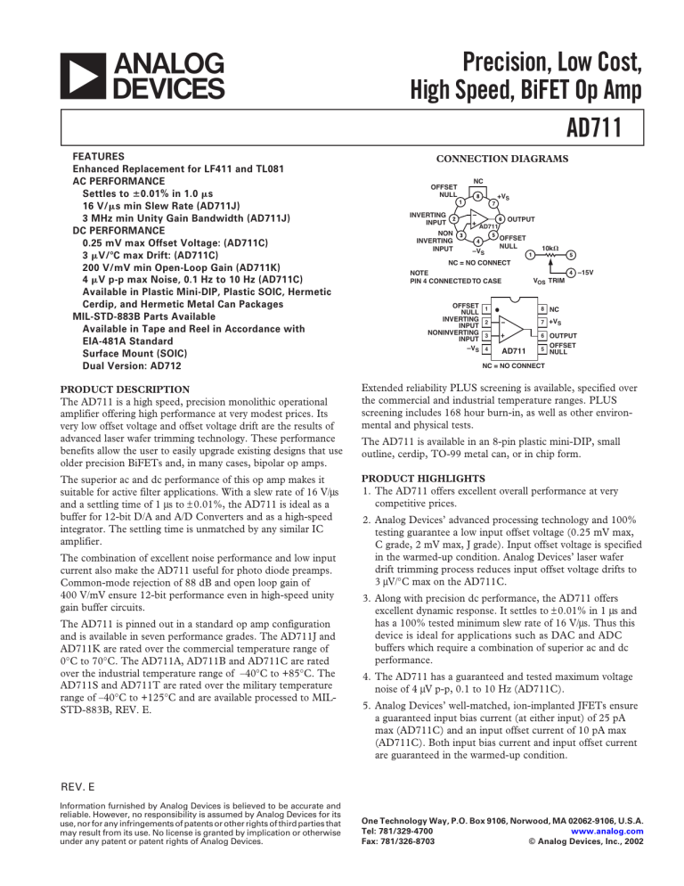
a FEATURES Enhanced Replacement for LF411 and TL081 AC PERFORMANCE Settles to ⴞ0.01% in 1.0 s 16 V/s min Slew Rate (AD711J) 3 MHz min Unity Gain Bandwidth (AD711J) DC PERFORMANCE 0.25 mV max Offset Voltage: (AD711C) 3 V/ⴗC max Drift: (AD711C) 200 V/mV min Open-Loop Gain (AD711K) 4 V p-p max Noise, 0.1 Hz to 10 Hz (AD711C) Available in Plastic Mini-DIP, Plastic SOIC, Hermetic Cerdip, and Hermetic Metal Can Packages MIL-STD-883B Parts Available Available in Tape and Reel in Accordance with EIA-481A Standard Surface Mount (SOIC) Dual Version: AD712 PRODUCT DESCRIPTION The AD711 is a high speed, precision monolithic operational amplifier offering high performance at very modest prices. Its very low offset voltage and offset voltage drift are the results of advanced laser wafer trimming technology. These performance benefits allow the user to easily upgrade existing designs that use older precision BiFETs and, in many cases, bipolar op amps. The superior ac and dc performance of this op amp makes it suitable for active filter applications. With a slew rate of 16 V/ms and a settling time of 1 ms to ± 0.01%, the AD711 is ideal as a buffer for 12-bit D/A and A/D Converters and as a high-speed integrator. The settling time is unmatched by any similar IC amplifier. The combination of excellent noise performance and low input current also make the AD711 useful for photo diode preamps. Common-mode rejection of 88 dB and open loop gain of 400 V/mV ensure 12-bit performance even in high-speed unity gain buffer circuits. The AD711 is pinned out in a standard op amp configuration and is available in seven performance grades. The AD711J and AD711K are rated over the commercial temperature range of 0∞C to 70∞C. The AD711A, AD711B and AD711C are rated over the industrial temperature range of –40∞C to +85∞C. The AD711S and AD711T are rated over the military temperature range of –40∞C to +125∞C and are available processed to MILSTD-883B, REV. E. Precision, Low Cost, High Speed, BiFET Op Amp AD711 CONNECTION DIAGRAMS OFFSET NULL NC +VS INVERTING INPUT OUTPUT AD711 NON INVERTING INPUT OFFSET NULL –VS 10k⍀ NC = NO CONNECT –15V NOTE PIN 4 CONNECTED TO CASE OFFSET NULL INVERTING INPUT NONINVERTING INPUT –VS VOS TRIM 1 8 NC 2 7 +VS 3 6 4 5 OUTPUT OFFSET NULL AD711 NC = NO CONNECT Extended reliability PLUS screening is available, specified over the commercial and industrial temperature ranges. PLUS screening includes 168 hour burn-in, as well as other environmental and physical tests. The AD711 is available in an 8-pin plastic mini-DIP, small outline, cerdip, TO-99 metal can, or in chip form. PRODUCT HIGHLIGHTS 1. The AD711 offers excellent overall performance at very competitive prices. 2. Analog Devices’ advanced processing technology and 100% testing guarantee a low input offset voltage (0.25 mV max, C grade, 2 mV max, J grade). Input offset voltage is specified in the warmed-up condition. Analog Devices’ laser wafer drift trimming process reduces input offset voltage drifts to 3 mV/∞C max on the AD711C. 3. Along with precision dc performance, the AD711 offers excellent dynamic response. It settles to ± 0.01% in 1 ms and has a 100% tested minimum slew rate of 16 V/ms. Thus this device is ideal for applications such as DAC and ADC buffers which require a combination of superior ac and dc performance. 4. The AD711 has a guaranteed and tested maximum voltage noise of 4 mV p-p, 0.1 to 10 Hz (AD711C). 5. Analog Devices’ well-matched, ion-implanted JFETs ensure a guaranteed input bias current (at either input) of 25 pA max (AD711C) and an input offset current of 10 pA max (AD711C). Both input bias current and input offset current are guaranteed in the warmed-up condition. REV. E Information furnished by Analog Devices is believed to be accurate and reliable. However, no responsibility is assumed by Analog Devices for its use, nor for any infringements of patents or other rights of third parties that may result from its use. No license is granted by implication or otherwise under any patent or patent rights of Analog Devices. One Technology Way, P.O. Box 9106, Norwood, MA 02062-9106, U.S.A. Tel: 781/329-4700 www.analog.com Fax: 781/326-8703 © Analog Devices, Inc., 2002
