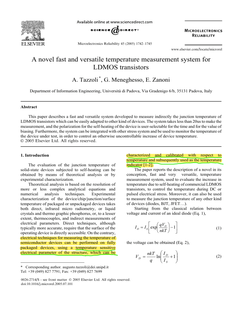
Microelectronics Reliability 45 (2005) 1742–1745 www.elsevier.com/locate/microrel A novel fast and versatile temperature measurement system for LDMOS transistors A. Tazzoli *, G. Meneghesso, E. Zanoni Department of Information Engineering, Università di Padova, Via Gradenigo 6/b, 35131 Padova, Italy Abstract This paper describes a fast and versatile system developed to measure indirectly the junction temperature of LDMOS transistors which can be easily adapted to other kind of devices. The system takes less than 20us to make the measurement, and the polarization for the self-heating of the device is user-selectable for the time and for the value of biasing. Furthermore, the system can be integrated with other stress system and be used to monitor the temperature of the device under test, in order to control an otherwise uncontrollable increase of device temperature. Ó 2005 Elsevier Ltd. All rights reserved. 1. Introduction The evaluation of the junction temperature of solid-state devices subjected to self-heating can be obtained by means of theoretical analysis or by experimental characterization. Theoretical analysis is based on the resolution of more or less complex analytical equations and numerical analysis techniques. Experimental characterization of the device/chip/junction/surface temperature of packaged or unpackaged devices takes both direct, infrared micro radiometry, or liquid crystals and thermo graphic phosphorus, or, to a lesser extent, thermocouples, and indirect measurements of electrical parameters. Direct techniques, although typically more accurate, require that the surface of the operating device is directly accessible. On the contrary, electrical techniques for measuring the temperature of semiconductor devices can be performed on fully packaged devices, using a temperature sensitive electrical parameter of the structure, which can be characterized and calibrated with respect to temperature and subsequently used as the temperature indicator [1-2]. The paper reports the description of a novel in its conception, fast and very versatile, temperature measurement system, used to evaluate the increase in temperature due to self-heating of commercial LDMOS transistors, to control the temperature during DC or pulsed electrical stress. Moreover, it can also be used to measure the junction temperature of any other kind of devices (diodes, BJT, JFET…). Starting from the classical relation between voltage and current of an ideal diode (Eq. 1), ID ª § qV · º I S «exp¨ D ¸ 1» ¬ © nkT ¹ ¼ (1) the voltage can be obtained (Eq. 2), * Corresponding author. augusto.tazzoli@dei.unipd.it Tel: +39 (049) 827 7791; Fax: +39 (049) 827 7699 0026-2714/$ - see front matter Ó 2005 Elsevier Ltd. All rights reserved. doi:10.1016/j.microrel.2005.07.101 VD · nkT § I D ln ¨¨ 1¸¸ q © IS ¹ (2) A. Tazzoli et al. / Microelectronics Reliability 45 (2005) 1742–1745 Fig. 1. Structure of a twin N-channel LDMOS. with the saturation current proportional to the intrinsic concentration of carriers ni2 (Eq. 3), I S v ni2 § E · BT 3 exp¨ G ¸ © kT ¹ (3) From the last equation, the heavy negative dependency of the voltage drop upon the diode with the increasing of the temperature is clear [3]. The basis of the thermal characterization is quite simple: i) any intrinsic diode present in the device (the Body-Drain diode in LDMOS) must be fully characterized at different temperatures; ii) the device is biased in order to produce self heating; iii) the intrinsic diode is hence used as a temperature probe by measuring the voltage drop consequent to self heating; comparing this voltage with a voltage-temperature map previously made in a climatic chamber it is possible to indirectly estimate the temperature of the device under test [4-6]; iv) the time between the end of the selfheating regime and the measuring of the intrinsic diode 660 1743 must be as short as possible in order to avoid device cooling down; v) the current adopted to measure the intrinsic diode must be as low as possible to avoid further self-heating. Figure 2 shows an example of calibration curve of the LDMOS intrinsic diode (BodyDrain) carried out at different temperatures. All devices tested exhibit the same behaviour and also very similar values for the calibration curve, despite differences in other electrical parameters. Usually, in thermal-characterization circuit proposed in literature, the measurement of the intrinsic diode following the self heating, [see iii) above], is biased at constant current. At the contrary, in order to simplify and make the measurement system as fast as possible, we have biased the diode at constant voltage limiting the current with a series resistor. The voltagetemperature conversion map takes into account the effect of the series resistor and in this way the system doesn’t need a successive calibration or correction session. It is important to note how to play with the results obtained with this kind of indirect temperature measurement, in particular with multi-finger devices. In fact, LDMOS transistors are constituted of several cells (for example, Ericsson PTF 10107A are constituted of 180 fingers), everyone with an intrinsic diode. During the calibration all diodes are at the same temperature, but being all diodes in parallel and because of the not probable equal self-heating of all the area of the device, the total current will be split between them as a function of their local temperature. For this reason, the measured temperature must not be A/D PIC CONVERTER 610 560 510 460 410 360 15 35 55 75 95 115 135 Temperature [ºC] Fig. 2. Example of a calibration curve for a LDMOS intrinsic diode. Interpolation clearly indicate a linear trend. PIC represent the output of the 10-bit AD converter of the adopted microcontroller. Fig. 3. Schematic of the temperature measure system. DUT is highlighted at the center of the scheme. 1744 A. Tazzoli et al. / Microelectronics Reliability 45 (2005) 1742–1745 70 40 60 1 0.8 30 0.6 Drain Voltage 20 Id [A] Vd [V] - Power [W] - Temp [°C] 50 1.2 0.4 Temperature [ºC] Polarization = 1.5ms Duty Cycle = 98.5% Vg = 5.8V 60 50 40 30 20 Temperature Dissipated Power 10 0.2 Drain Current 0 000E+0 20E-3 10 Duty Cycle = 82% Duty Cycle = 90% Duty Cycle = 95.7% Duty Cycle = 97.8% Duty Cycle = 98.5% 0 0 40E-3 Room Temperature 60E-3 80E-3 100E-3 120E-3 Time [s] Fig. 4. Measurement of the junction temperature, Vd, Id, and dissipated power for an open-package LDMOS biased with a Duty Cycle of 98.5% for the first 60ms and then left cooling. considered the true temperature but a temperature between the maximum and the average one. 2. Measurement system description The measurement system is constituted by a Hp 8114A pulse generator, a Hp 3631A power supplier, a pc, and a self-made circuit that controls all the operations of the system, see Figure 3. The heart of the circuit is based on the Microchip PIC 16F877A. The microcontroller, clocked at 20Mhz, controls the correct synchronization between the energy pulse, provided by the pulser used in External Trigger Mode and the power supplier, and the measurement of the device temperature by switching two opto-couplers and a NMOS transistor. In this way, it is possible to bias a device at any values of Drain and Gate voltage, and for any time, starting from some hundreds of nanoseconds to hours, at the contrary of others more limited circuit presented in literature. In addition, the circuit was designed to allow the polarization of the device not only with square shaped energy pulses, but with any shaped ones, using an arbitrary waveform generator, usually amplified for power pulses. This feature can be useful to run the measurement with triangular shaped pulse to obtain inductive like self-heating or other behaviours [4]. The internal A/D converter of the microcontroller is also used to measure the Drain and the Source voltage during the energy pulse. Only in 20 us the 000E+0 25E-3 50E-3 75E-3 100E-3 125E-3 Time [s] Fig. 5. Comparison between different value of Duty Cycle for the polarization of the same transistor. microcontroller makes the result and, thanks to its 10 bits resolution, the temperature can be evaluated with a better resolution compared to other systems based to classical 8 bits Digital Oscilloscope. Furthermore, the current flowing through the device is measured by the voltage drop up a 1 ohm sense resistor. In this way it is possible to evaluate the instantaneous power dissipated by the device and so the self-heating. A very important feature of this system is the very short time spent to switch between the self-heating stage and the temperature measurement one. In fact, the measurement must be performed as fast as possible after the energy pulse, otherwise, especially dealing with short pulse, the device could have enough time to cooling itself too much. The microcontroller only in 200 nanoseconds control the switches and, considering the switching time of the NMOS and of the two optocouplers, the temperature measurement is not delayed more than 1 us. This guarantees that the temperature measurements are far less than one unit per cent from the real values. The circuit is controlled by a pc through the parallel port, used also to transfer the measured value to the pc. The program, written in Visual Basic, is used to set the duration of the energy pulse, the waiting time between two measurement and the number of average and to ease the construction of the calibration plot. Furthermore, to avoid boring data manipulation, the program is able to communicate with a spreadsheet to create the graph of the measured value of temperature, Drain-Source voltage, current and power dissipated. Another feature of the system is its capability to stop the polarization if the temperature goes over a preset value. This feature can be used to monitor the junction temperature of the device during long DC stress and A. Tazzoli et al. / Microelectronics Reliability 45 (2005) 1742–1745 65 160 Original Package Open Package 60 1745 140°C limit point 140 120 50 45 DC = 98.5% 40 DC = 95.7% 35 30 Vg = 5.8V Dissipated Power = 7.8W 25 20 000E+0 25E-3 50E-3 75E-3 100E-3 125E-3 Time [s] Temperature [°C] Temperature [ºC] 55 100 Vg = 5.8V Vd = 35V Id = 400mA Power = 14W 80 60 40 20 Ambient Temperature = 24°C 0 0 2000 4000 6000 8000 10000 Time [ms] Fig. 6. Comparison between original and open-package LDMOS biased with Duty Cycle of 95.7% and 98.5%. can be very helpful to avoid self-destruction due to an excessive self-heating. 3. Measurements Figures 4 to 7 depict several plot of the increase of the junction temperature during the self-heating stage and during the following cooling. LDMOS tested were either in closed package or in opened one, in order to evaluate the differences in the heating and the influence of the package. As expected open-package devices dissipate the heat better than packaged ones, but the difference is not so pronounced. All measures were made biasing the Gate of the device under test at 5.8V and the Drain at about 18V in order to make the transistor dissipate about 7.8W. The duration of the energy pulse was instead variable and, being the duration of the temperature measurement fixed to about 20us, the corresponding duty cycle starts from about 80% to about 99%. In the last case, depicted in Figure 7, the LDMOS can be considered stressed like in a DC stress, but when the temperature reached the preset maximum value, 140°C in this case, the system turned off the power and left the device to self-cooling to avoid self-destruction. 4. Conclusions We have developed a new system capable to indirectly measure the device temperature which have the following main advantages with respects to other already presented in literature: i) higher resolution in temperature, Vd, and Id measurements; ii) fast speed in Fig. 7. The measurement system can automatically stop the biasing when the temperature goes over a preset value. In this case the preset value was set at 140°C. the switching topology stage (self-heating/temperature measurements); iii) fast speed in temperature measurement; iv) adaptability with any devices which present an intrinsic diode; v) possibility of integrate this circuit with other electrical stress system in order to monitor and limit the maximum temperature. References [1] J. C. Whitaker, “The Electronics Handbook, Heat Management”, CRC Press, IEEE Press, pp. 1133-1157 [2] R.Menozzi, J. Barrett, P. Ersland, A. Kingswood, “New Methods for Easy DC Extraction Of The Thermal Resistance Of Microwave Bipolar and FET Devices”, Proceedings from WOCSDICE 2005, Session 4, pp. 8991. [3] R. S. Muller, T. I. Kamins, “Device Electronics for Integrated Circuits, 3rd edition”, Ed. Wiley, 2003, pp. 15–64. [4] J.M. Bosc, P. Dupuy, J. Gil, J.M. Dorker, G. Sarrabayrouse, “Thermal characterization of LDMOS transistors for accelerating stress testing”, Microelectronics Journal n. 31, 2000, pp. 747-752. [5] Application Note: “Transient Thermal Resistance – General Data And Its Use” , AN569, Motorola Semiconductor Products Inc. [6] Application Note: “Basic Semiconductor Thermal Measurement”, AN1570, Motorola Semiconductor Products Inc.


