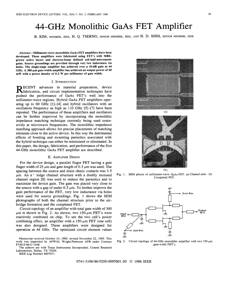
IEEE ELECTRON DEVICE LETTERS, VOL. EDL-7, NO. 95 2 , FEBRUARY 1986 44-GHz Monolithic GaAs FET Amplifier B. KIM, MEMBER,IEEE, H. Q . TSERNG, SENIORMEMBER,IEEE,AND H.D. SHIH, SENIORMEMBER,IEEE Abstract-Millimeter-wave monolithic GaAs FET amplifiers have been developed. These amplifiers were fabricated using FET’s with MBEgrown active layersand electron-beam defined sub-half-micrometer gates. Source groundings are provided through very low inductance via boles. The single-stage amplifier has achieved over a 10-dB gain at 44 GHz. A 300-pm gate-width amplifier has achieved an output power of 60 mW with a power density of 0.2 W per millimeter of gate width. I. INTRODUCTION R ECENT advances in material preparation, device fabrication, and circuit implementation techniques have pushed the performance of GaAs FET’s well into the millimeter-wave regions. Hybrid GaAs FET amplifiers operating up to 60GHz [1]-[41 andhybrid oscillators with an oscillation frequency as high as 110 GHz [5]-[7] have been reported. The performance of these amplifiers and oscillators can be further improved by incorporating themonolithic impedancematchingtechnique currently being used extensively at microwave frequencies. The monolithic impedance matching approach allowsfor precise placements of matching elements close to the active device. In this way the detrimental effects of bonding and mounting parasitics associatedwith the hybrid technique caneither be minimized or eliminated. In this paper, the design, fabrication, and performance of the first 44-GHz monolithic GaAs FET amplifier are described. 11. AMPLIFIER DESIGN For the device design, a parallel finger FET having a gate finger width of 25 pmand gate length of 0.3 pm was used. The spacing between the source and drain ohmic contacts was 3.5 pm. An n ledge channel structure with a doubly recessed channel region [SI wasused to reduce the parasitics and to maximize the device gain. The gate was placed very close to the,source with a gapof under 0.5 pm. To further improve the gain performance of the FET, very low inductance via holes wereused for sourcegroundings. Fig. 1 shows the SEM photographs ofboth the channel structure prior to the airbridge formation and the completed FET. Circuit topology of an amplifier with total gate width of 300 pm is shown in Fig. 2. As shown, two 150-pm FET’S were reactively combinedon chip. To see the two cell’s power combining effect, an amplifier with a 150-pm FET (one cell) was also designed.These amplifiers weredesigned for operation at 44 GHz. The optimized circuit element values + Manuscript received October 10, 1985; revised November 22, 1985. This workwassupported by AFWAL Wright-Patterson AFB underContract F33615-84-C-1448. The authors are with Texas Instruments Incorporated, Central Research Laboratories, Dallas, TX 75265. IEEE Log Number 8407071. (b) Fig. 1. SEM photos of millimeter-waveGaAsFET.(a)Channelarea. Completed FET. (b) 0 output 50 n c-0 GateBias I Fig. 2. Circuit topology of 44-GHz monolithic amplifier with two 150-pm gate-width FET’s. 0741-3106/86/0200-0095$01.OO O 1986 IEEE IEEE ELECTROK DEVICE LETTERS, VOL. EDL-7, KO.2, FEBRUARY 1986 96 were obtained by a conventional computer optimization technique using FET models generated from S-parameter measurements at lower frequencies. A characteristic impedance of 85 D was used for the transmission lines. 111. CIRCUIT FABRICATION Fig. 3 shows the two completed amplifiers. The chip sizes are 24 x 54 x 4 mil and 28 x 60 x 4 mil, respectively. The substrates used in this work were 2-in-diameter Cr-doped LEC slices. The epitaxial layers were grown by the PerkinElmer 425B molecular beam epitaxy (MBE) system. The material structure is comprised of three epitaxial layers: a 1pm undoped buffer layer; a0.3-pm n-GaAs active layer doped to 4.2 X 10i7/cm3;and a0.1-pm n - GaAs contact layer doped to about 5 X 101s/cm3. The doping transition at the interface between the n-layer andthe buffer layer has a maximum slope of about 0.030 pm/decade. Following the epitaxial layer growth, mesas were etched to isolate FET's and AuGe/Ni/Au ohmic contacts were formed. The wide recess pattern ( 1.5 pm wide) of the n ledge structure was then defined in PMMA by electron beam lithography and the channel was etched through the n layer into the n layer. The 0.3-prn gate pattern is then similarly defined in a 0.5-pm-thick layer of PMMA and the GaAs is etched again down to the final desired saturation current value. The 0.5-pm-thick Ti/Pt/Au gates were then fabricated. The same set of alignment marks was used for both the wide recess and the gate definition. A1.6-pm-thick Au layer wasthen evaporated and lifted off to produce the capacitor bottom plates, the inductors and the source grounding pads. MIM capacitors were fabricated, with 0.4-pm-thick silicon nitride as a dielectric. Then plated gold air bridges for contacting FET sources and capacitor top plates were formed. Transmission lines and all pads were plated with 3 pm of gold at the same time. The slice was then lapped to a thickness of 100 pm. Grounding vias (2 mil x 3 mil) were etched by the reactive ion etching technique. A 10-pm-thick platedgold heat sink interconnects all the vias. IV , MICROWAVE PERFORMANCE - + (b) Fig. 3. Photographs of completed 44-GHz monolithic amplifiers. (a) Amplifier with 150-pm gate-width FET. (b) Amplifier with 300-prn gate- width FET. + '..p h :::I, 1:: - The measured gain-frequency responses of the amplifiers are shown in Fig. 4.Without any external tuning, the 150-pm device has a 9.5-dB gain centered at 43 GHz. When the output was tuned, the gain was increased to 11 dB. A 300-pm amplifier achieved more than a 10-dB gain across the 44-46 GHz band, without any tuning. The power saturation characteristics of these amplifiers were also tested at 44 GHZ. Fig. 5 shows the measured results. The 150-pm amplifier delivered 30 mWof output power with a 6-dB gain and 7-percent efficiency. A drain bias of 5 V and a gate bias of - 0.1 V were used for the results shown in Fig. 5. The 300-pm amplifier generated 60 mW of power with a 5-dB gain. The corresponding power density is 0.2 W/mm. It is seen that there is no performance degradation caused by the two cell combining. With further device optimization, an output power density of at least 0.5 W/mm can be expected. V. CONCLUSIONS Monolithic millimeter-wave GaAs FET amplifiers with subhalf-micrometer gates have been designed, fabricated, and RF , 0.0 41 .O I , , , I 42.0 FREPUEXY , I I 43.0 (GHZ) , ! , 44.0 I 0.0 (a) -1 0 43 44 45 FREQUENCY (GHz) 46 47 (b) Fig. 4. Gain frequency response of W G H z monolithic amplifiers. (a) 150pm gate-width FET. (b) 300-pm gate-width FET. 97 KIM et al. : GaAs FET AMPLIFIER ACKNOWLEDGMENT The authors would like to thank K. Bradshaw and S . Meyer for the electron beam lithography. For technical assistance they thank B. Clark, S . F. Goodman, J . M. Ramzel, and P. A. Tackett. REFERENCES 5-Z 0 2 4 6 E 10 INPUT POWR (dBrn) Fig. 5 . Gain compression characteristics of the 150-pm FET amplifier. tested. Amplifiers with gate widths of 150 and 300 pm have achieved over a 10 dB gain at 44 GHz. This is the first report of the monolithic implementation of GaAs FET amplifiers above 40 GHz. These excellent gain results were achieved by the use of submicrometer gate FET andoptimized circuit topology. Even though the power density is a modest 0.2 WI mm, these results show that monolithic GaAs FET amplifier is a viable millimeter-wave active component useful for system applications. With further device optimization, it is believed that the power density can be further improved to at least 0.5 Wlmm of gate width. P. W. Chye and C. Huang, “Quarter micron low noise GaAs FET’s,” ZEEE Electron Device Lett., vol. EDL-3, pp. 401-403, Dec. 1982. E. T. Watkins, J . M. Schellenberg, L. H. Hackett, H. Yamasaki, and M. Feng, “A 60-GHz GaAs FET Amplifier,” in 1983 ZEEE Microwave Theory Tech. Symp. Dig., June 1983, pp. 145-147. M.Feng, H. Kanber, V. K. Eu, E. Watkins, and L. R. Hackett, “Ultrahigh Frequency Operation of Ion-Implanted GaAs Metal-Semiconductor Field-Effect Transistors,” Appl. Phys. Lett., vol. 44, no. 2, pp. 231-233, Jan. 1984. [41 8.Kim, H. Q. Tserng, andH. D. Shih, “Millimeter-wave GaAs FETs prepared by MBE,” ZEEE Electron Device Lett., vol. EDL-6, pp. 12, Jan.1985. H. Q . Tserng and B. Kim,“High Efficiency Q-Band GaAs FET Oscillator,” Electron. Lett., vol. 20, no. 7, pp. 297-298, Mar. 1984. D. W. Maki, J . M. Schellenberg, H. Yamasaki, and L. C. T. Liu, “A 69-GHz monolithic FET oscillator,” in ZEEE 1984 Microwave and Millimeter- Wave Monolithic Circuits Symp. Dig., pp. 62-66. H. Q. Tserngand B. Kim, “110 GHz GaAs FET oscillator,” Electron. Lett. vol. 21, no. 5 , pp. 178-179, Feb. 1985. H. M. Macksey and R. D. Hudgens, “Fabrication of n ledge channel structure for GaAs FET’s with a single lithography step,” E/ectron. Lett., vol. 21, no. 7, pp. 955-957, Oct. 1985. +


