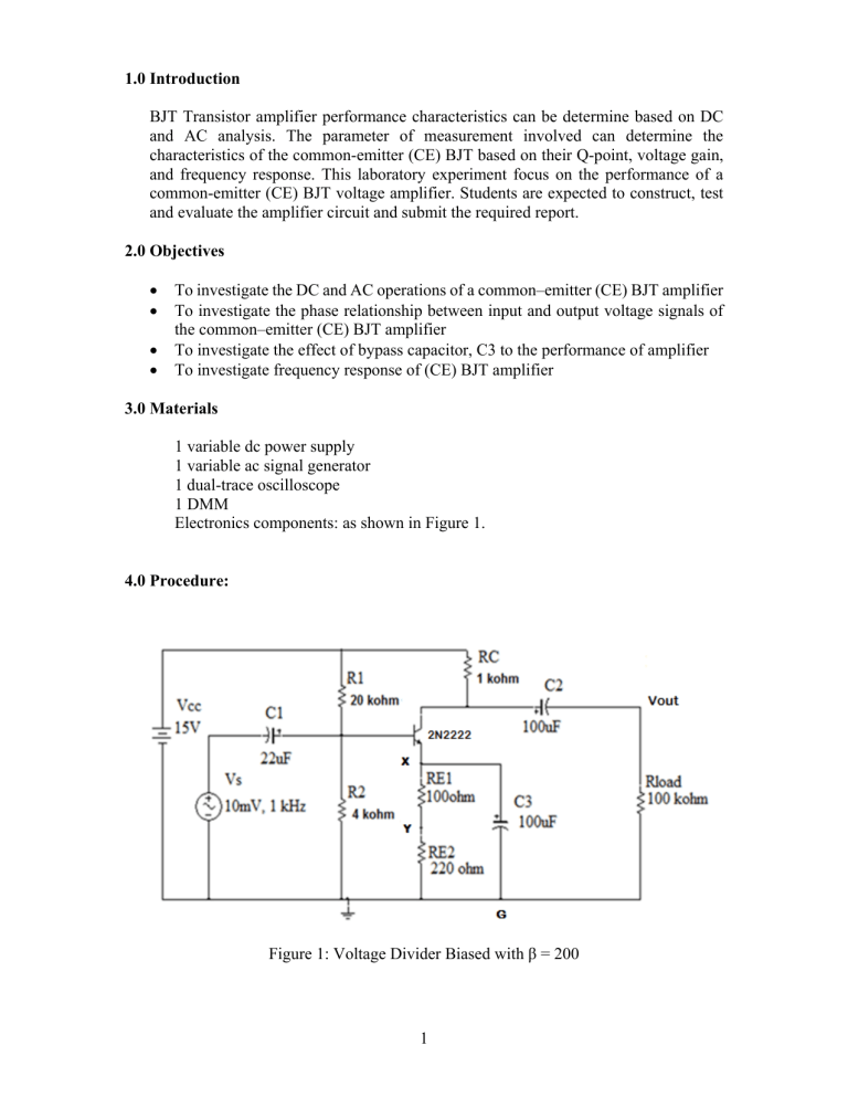
1.0 Introduction BJT Transistor amplifier performance characteristics can be determine based on DC and AC analysis. The parameter of measurement involved can determine the characteristics of the common-emitter (CE) BJT based on their Q-point, voltage gain, and frequency response. This laboratory experiment focus on the performance of a common-emitter (CE) BJT voltage amplifier. Students are expected to construct, test and evaluate the amplifier circuit and submit the required report. 2.0 Objectives To investigate the DC and AC operations of a common–emitter (CE) BJT amplifier To investigate the phase relationship between input and output voltage signals of the common–emitter (CE) BJT amplifier To investigate the effect of bypass capacitor, C3 to the performance of amplifier To investigate frequency response of (CE) BJT amplifier 3.0 Materials 1 variable dc power supply 1 variable ac signal generator 1 dual-trace oscilloscope 1 DMM Electronics components: as shown in Figure 1. 4.0 Procedure: Figure 1: Voltage Divider Biased with β = 200 1 TASK 1: Refer to the circuit shows in Figure 1. (Student Name: ____________________________________________) (Student ID: _______________________________________________) 1. Convert the circuit in Figure 1 into re equivalent circuit. 2. Determine Zi and Zo 3. Determine Av and Ai 4. Calculate ICQ and VCEQ 5. IC and VCE at the point of saturation and cutoff Under DC operation Under AC operation 6. The AC and DC load lines 7. Quiescent Power 8. AC Output Power 9. Efficiency (25 marks) 2 TASK 2: Refer to the circuit shows in Figure 1. (Student Name: ____________________________________________) (Student ID: _______________________________________________) 1. Obtain the value of β of BJT transistor 2N2222A from the datasheet. Datasheet Value β (1 marks) 2. Using multisim, construct the circuit as shown in Figure 1. a) Apply 15 V, Vcc to the circuit, measure (using multimeter) and record the values of VC, VE ,VCE and IC Measurement point VC Value VE VCE IC [8 marks] b) Apply a 1-kHz, 20mV(p-p) ac signal (Vs) as the input of the amplifier. c) Measure and record the peak-to-peak input and output voltages of the amplifier. Measurement point Vs Value (Vp-p) Vout [4 marks] 3 Draw the input and output voltage waveforms vs time on the grid provided in Figure 2. Starting time for both waveforms must be same. Note on the phase relationship between input and output signal. V/div : _________________ Time/Div: _________________ V/div: _________________ Time/Div: _________________ [6 marks] Figure 2 d) Calculate the voltage gain of the amplifier in numerical and dB. Show your calculations. AVnumerical = [3 marks] 4 AVdB = [3 marks] 5 TASK 3: Refer to the circuit shows in Figure 1. (Student Name: ____________________________________________) (Student ID: _______________________________________________) 1. Using multisim, construct the circuit as shown in Figure 1. Apply 15 V, Vcc to the circuit. Apply a 1-kHz, 20mV(p-p) ac signal (Vs) as the input of the amplifier. a) Change the connection of C3 from G-X to G-Y and determine the new Vop-p and Av of the amplifier. Measurement point Vop-p Value Av [5 marks] b) Varies the input frequencies as shown in Table 1 and fill in the values of respective output voltage and the voltage gain. Vs (p-p) 20 mVp-p Table 1 Input Frequency (Hz) 10 50 100 400 600 800 900 1K 2K 5K 10K 15K 20K 30K 40K 60K 70K 80K 100K 400K 600K 6 Vout (p-p) Av = Vout / Vin 800K 1M 2M [10 marks] c) Plot the frequency response graph using semi-log paper with complete labels [5 marks] d) Use the frequency response to determine:Avmax = fCH = fCL = BW = fCH – fCL = [5 marks] TASK 4: Perform analysis and conclusion in video presentation format form (.avi) and submit video link to respective lecturer. (Student Name: ____________________________________________) (Student ID: _______________________________________________) 1. Analyze the results obtained from Task 2 and Task 3. Comment on the following focusing area: Position of the Q point on the DC load line. The amount of voltage amplification The phase relationship between input and output voltages Effect of bypass capacitor, C3 on the voltage gain The frequency response of the amplifier 2. The conclusion of this experiment. [25 marks] 7


