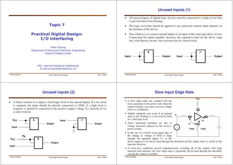
Unused inputs (1) Topic 7 Practical Digital Design: I/O interfacing Peter Cheung Department of Electrical & Electronic Engineering Imperial College London URL: www.ee.imperial.ac.uk/pcheung/ E-mail: p.cheung@imperial.ac.uk PYKC 8-Feb-08 E3.05 Digital System Design Topic 7 Slide 1 PYKC 8-Feb-08 Unused inputs (2) PYKC 8-Feb-08 E3.05 Digital System Design E3.05 Digital System Design Topic 7 Slide 2 Slow Input Edge Rate Topic 7 Slide 3 PYKC 8-Feb-08 E3.05 Digital System Design Topic 7 Slide 4 Avoid floating inputs PYKC 8-Feb-08 E3.05 Digital System Design Simultaneous Switching Outputs (1) Topic 7 Slide 5 PYKC 8-Feb-08 Simultaneous Switching Outputs (2) PYKC 8-Feb-08 E3.05 Digital System Design E3.05 Digital System Design Topic 7 Slide 6 Ground Bounce (1) Topic 7 Slide 7 PYKC 8-Feb-08 E3.05 Digital System Design Topic 7 Slide 8 Ground Bounce (2) PYKC 8-Feb-08 Ground Bounce (3) Topic 7 Slide 9 E3.05 Digital System Design Capacitive Loads or Transmission Line (1) PYKC 8-Feb-08 E3.05 Digital System Design Topic 7 Slide 11 PYKC 8-Feb-08 E3.05 Digital System Design Topic 7 Slide 10 Capacitive Loads or Transmission Line (2) PYKC 8-Feb-08 E3.05 Digital System Design Topic 7 Slide 12 Bus Contention PYKC 8-Feb-08 E3.05 Digital System Design Pullup or Pulldown resistors Topic 7 Slide 13 PYKC 8-Feb-08 Bus Hold Circuit PYKC 8-Feb-08 E3.05 Digital System Design E3.05 Digital System Design Topic 7 Slide 14 Bus Hold Circuit Topic 7 Slide 15 PYKC 8-Feb-08 E3.05 Digital System Design Topic 7 Slide 16 Series Damping Resistor (1) PYKC 8-Feb-08 E3.05 Digital System Design Series Damping Resistor (2) Topic 7 Slide 17 PYKC 8-Feb-08 Here is a summary of different terminations that may be programme on a typical FPGA I/O block (example taken from Xilinx). X X Modern digital electronics use many different I/O standards. Here is an incomplete list: • • • • • • • • • • X PYKC 8-Feb-08 E3.05 Digital System Design Topic 7 Slide 19 Topic 7 Slide 18 Modern Electronics I/O Standards FPGAs provides many of these functions (1) X E3.05 Digital System Design LVTTL – Low-voltage TTL LVCMOS2 – Low-voltage CMOS for 2.5v PCI – Peripheral Component Interface GTL – Gunning Transceiver Logic (Terminated) GTL+ - Gunning Transceiver Logic Plus HSTL – High-Speed Transceiver Logic SSTL2 – Stub Series Terminated Logic for 2.5v SSTL3 – Stub Series Terminated Logic for 3.3v LVDS – Low Voltage Differential Signals AGP – Advanced Graphics Port The following specifications of these standards refer to those used by Xilinx in their Virtex family of FPGAs. PYKC 8-Feb-08 E3.05 Digital System Design Topic 7 Slide 20 Types of I/O X Uni-direction buffer X Tri-state buffer X Bi-direction I/O buffer X Open-drain interface PYKC 8-Feb-08 X LVTTL — Low-Voltage TTL X Differential interfaces X E3.05 Digital System Design Topic 7 Slide 21 PYKC 8-Feb-08 LVCMOS2 — Low-Voltage CMOS for 2.5 Volts X X The LVCMOS2 standard is an extension of the LVCMOS standard used for general purpose 2.5V applications. It uses a 5V tolerant CMOS input buffer and a Push-Pull output buffer. This standard requires a 2.5V output source voltage (VCCO), but does not require the use of a reference voltage (VREF) or a board termination voltage (VTT). PYKC 8-Feb-08 E3.05 Digital System Design Topic 7 Slide 23 The LVTTL standard is a general purpose EIA standard for 3.3V applications that uses an LVTTL input buffer and a Push-Pull output buffer. The input and output buffers are both 5V-tolerant. This standard requires a 3.3V output source voltage (VCCO), but does not require the use of a reference voltage (VREF) or a termination voltage (VTT). E3.05 Digital System Design Topic 7 Slide 22 GTL — Gunning Transceiver Logic Terminated X X The GTL standard is a high-speed bus standard invented by Xerox. Many FPGA companies have implemented the terminated variation for this standard, requiring a differential amplifier input buffer and a Open Drain output buffer. PYKC 8-Feb-08 E3.05 Digital System Design Topic 7 Slide 24 GTL+ — Gunning Transceiver Logic Plus X HSTL — High-Speed Transceiver Logic The GTL+ standard is a high-speed bus standard derived from GTL, first used by the Pentium Pro processor. X X PYKC 8-Feb-08 E3.05 Digital System Design Topic 7 Slide 25 The HSTL standard is a general purpose high-speed, 1.5V bus standard sponsored by IBM and has four variations or classes. This standard requires a Differential Amplifier input buffer and a Push-Pull output buffer. PYKC 8-Feb-08 SSTL3 — Stub Series Terminated Logic for 3.3V X X X E3.05 Digital System Design Topic 7 Slide 26 SSTL3 — Stub Series Terminated Logic for 3.3V A general purpose 3.3V memory bus standard sponsored by Hitachi and IBM. This standard has two classes, I and II. This standard requires a Differential Amplifier input buffer and an Push-Pull output buffer. PYKC 8-Feb-08 E3.05 Digital System Design X X X Topic 7 Slide 27 A general purpose 3.3V memory bus standard sponsored by Hitachi and IBM. This standard has two classes, I and II. This standard requires a Differential Amplifier input buffer and an Push-Pull output buffer. PYKC 8-Feb-08 E3.05 Digital System Design Topic 7 Slide 28 LVDS – Low voltage differential signal (1) SSTL2 — Stub Series Terminated Logic for 2.5V X X The SSTL2 standard is the same as SSTL3, but for 2.5V. There are also two classes: I & II. X X PYKC 8-Feb-08 E3.05 Digital System Design Topic 7 Slide 29 This is a fully differential signals often used for very high speed network connections. The transmit and receive circuits are different. PYKC 8-Feb-08 LVDS – Low voltage differential signal (2) Other programmable features (in addition to termination) are: • • • • • • • E3.05 Digital System Design Topic 7 Slide 30 FPGAs provides many of these functions (2) X PYKC 8-Feb-08 E3.05 Digital System Design Topic 7 Slide 31 Input Reference Voltage (Vref) Output Source Voltage (Vcco) Board Termination Voltage (Vtt) Output Slew Rate Output Drive Strength Synchronous/Asynchronous I/O Programmable Output Delay (called ChipSynch in Xilinx) PYKC 8-Feb-08 E3.05 Digital System Design Topic 7 Slide 32 Xilinx Virtex 5 I/O capability Altera Cyclone-II I/O Features Each pin can be input and ( 3-state-able) output Each pin can be individually configured for: X X • ChipSync, XCITE termination, drive strength, input threshold, weak pull-up or down X Each input can be 3.3-V tolerant, limited by its Vcco X Each I/O can have the same performance X Each I/O supports 40+ voltage and protocol standards including: • No 5-V tolerance, unless current-limiting R is used • Up to 700 Mbps single-ended & 1.25 Gbps differential LVDS X X X X X LVCMOS (3.3v, 2.5v, 1.8v, 1.5v, and 1.2v) LVDS, Bus LVDS, Extended LVDS LCPECL PCI, PCI-X HyperTranport (LDT) PYKC 8-Feb-08 X X X X X HSTL (1.8v, 1.5v, Classes I, II, III, IV) HSTL_I_12 (unidirectional only) DIFF_HSTL_I_18, DIFF_HSTL_I_18_DCI DIFF_HSTL_I, DIFF_HSTL_I_DCI RSDS_25 (point-to-point) X X X X X E3.05 Digital System Design SSTL (2.5v, 1.8v, Classes I, II) DIFF_SSTL_I DIFF_SSTL2_I_DCI DIFF_SSTL18_I, DIFF_SSTL18_I_DCI GTL, GTL+ Topic 7 Slide 33 Useful References X X X Application Notes SDYA009C, “Designing with Logic”, Texas Instrument, June 1997. XAPP133, “Using the Virtex Select I/O Resource”, Xilinx. Cyclone II Device Handbook, Vol. 1, p. 2-37 to 2-61. PYKC 8-Feb-08 E3.05 Digital System Design Topic 7 Slide 35 PYKC 8-Feb-08 E3.05 Digital System Design Topic 7 Slide 34


