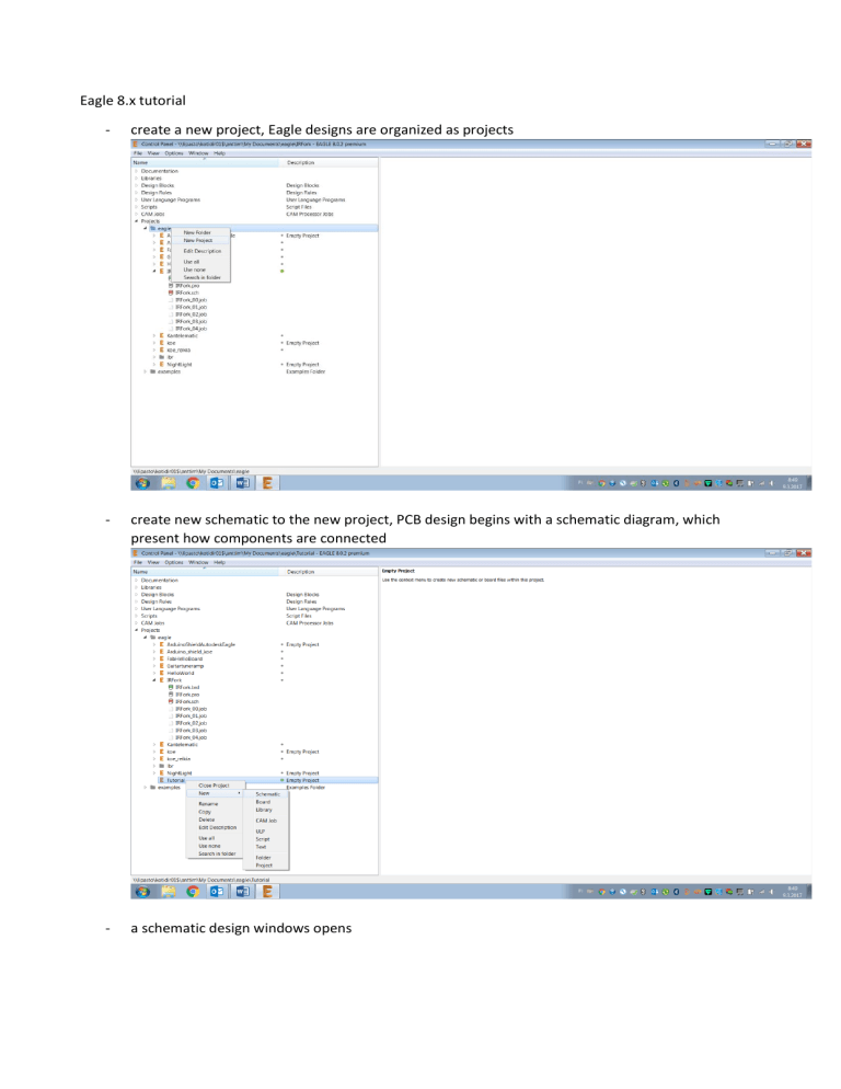
Eagle 8.x tutorial - create a new project, Eagle designs are organized as projects - create new schematic to the new project, PCB design begins with a schematic diagram, which present how components are connected - a schematic design windows opens - add components to the schematic - there might be shown some or all available component libraries, components are organized in libraries by their type or provider fab-library (file fab.lbr) contains the components typically used in Fab Lab supply1-library contains power supply symbols such as GND (0V) and VCC (+, positive voltage) - - if you need other components not found in the libraries shown, clock USE - a file manager window opens and shows available components - you can keep your own libraries and the libraries you have downloaded (such as adafruit or sparkfun) in the folder you want - add library paths to the directories setting - let’s add GND, VCC, resistor, capacitor, integrated circuit and a connector… by pressing esc you get back to the ADD-operation - RES-US1206FAB is a good choice for a resistor, because it has room to route a connection under the component (as all components with FAB suffix) - many integrated circuits have package variations, we choose surface mount small outline - the component we have has 6 NOT-gates in a single package, and we must add them one by one - and press esc when all gates have been inserted, otherwise we are adding the next component as the connector we use 2x2 surface mount pin header - - the next thing to do is to place the components in a logical order, in my circuits the signal flow is usually from left to right the components are moved with the move-command, point the cursor to the + symbol in a component, then press left button and drag when over the component + symbol mouse right clock opens a menu for available operations, such as rotate the integrated circuit has no visible power supply pins, but it is defined in the library component that pin 14 connects to VCC and pin 7 to GND - the component are connected with the operation Net - point a component pin and left click to begin a net, add corners with left click and end the net to a component pin or net intersection - net net can also begin without a pin, and a double left click end the net - connect all nets… let’s also rename the connector - with everything connected the schematic should look like this. The unused inputs of the CMOS logic gates must be connected to GND or VCC depending the function of the unused pins, this time GND is OK. http://www.radio-electronics.com/info/circuits/logic-digital-design-guidelines-tips/logicunused-gate-input-termination.php - then perform ERC (Electrical Rules Check) to your circuit - we forgot to give value to the resistor (actually capacitor has no value either), the output of the unused gates are unconnected, but that is OK, they are unused, don’t connect them anywhere! - let’s give a value to the resistor - say 10k (Ohms), capacitor can be 100n (Farads) - when the schematic is finished, let’s switch to the board design - click yes and a new window opens change grid to mm units the default routing grid is 1.27 mm, but you can halve it while routing with the alt-button - and make the board smaller, the default board size is 160x100 mm, just left click the board outline and drag the vertical and horizontal lines, keep the origin in the lower left corner - then place the components inside the board outline. This is a critical phase! The layout of the components determines how easy it is the route the physical copper connections (nets) between the components - you should try to reach a layout in which the length of the connections is as short as possible with as few lines crossing as possible after modifying the placement of the components press Ratsnest to recalculate the connecting wires (ratsnest) - the components are moved with the Move command, point the cursor to the + symbol of the component and left click and drag - components can be rotated also with the Rotate command - a couple of other useful operations: zoom with mouse roller press middle button/roller and move mouse to pan - now with everything in place let’s start routing - but first make some settings: a good value for routing isolation between wires is 0.4064 mm (16 mil, 1/1000 inch) - good copper width is also 0.4064 mm - some settings for Design Rule Check (DRC) are also needed - change 16mil to all - change 16mil here too - thermal pad spoke width 16mil - now we are all set for routing… start a new route with left click, change the routing angle with right click, halve the routing grid with alt-button if needed, and end the route with left click - then with everything else routed but GND, draw a polygon around the board. This polygon is used to automatically generate a so called copper pour to which all pins connected to GND net are connected - start the polygon with a left click, add corners with left click and end the polygon to the start point with a left click - the finished polygon is made of a dotted line name the polygon GND to connect it to the GND net - then press Ratsnest, and the copper pour appears - the board was slightly too small to surround the VCC with GND copper pour, so stretch it and Ratsnest again - perform DRC - and if no errors, happy times! - mounting holes might be needed in the Fab Lab PCB process, a circle with the line width of 0.99 mm drawn on Milling layer 46 is fine, because the process starts with bitmap pictures, we don’t use actual drilling files with tools and coordinates a circle without the hole might be better and safer to the milling tool… - - after adding the vias and moving components to make room for the vias, some routes need cleaning with the Ripup-tool, which removes routed segments The board is ready for manufacturing. - for this one-sided board we need a picture of the copper with layer select, select only layer 1 Top visible - then export image - with these settings (2400 dpi might be overkill…), but make it monochrome - the png-image looks like this, and it is too wide, the width is determined by the widest object in the design - I had to change the value of the connector to shorten the name to fit within the board boundaries - a new try with the image - I also drew a 0.99 mm line around the board in Milling layer 46, this line is used for milling the pcb loose from the larger copper blank changed the user interface background white - - the outline image is exported with white background, 1500 dpi is enough with the outline whereas the copper image is exported with black background the final png images for copper traces and outline look like that check that the dimensions match - Fabrication with Roland SRM-20 milling machine open fabmodules.org website - select input format image .png-file - select output format to Roland mill - select process to PCB traces (1/64) (inches = 1/64 * 25.4 = 0.39 mm) - choose machine and check the other parameters - then press calculate and the tool path are created save the .rml file with the save button - then create the tool paths for milling the outline and holes again select Roland Mill - the process is PCB Outline (1/32) (inches-> 1/32 * 25.4 = 0.79 mm) - check the parameters and press calculate you can rotate the milling picture by pressing and holding mouse right button to see, that the milling tool makes 3 passes with different depths press save to save the .rml-file - What if you have through hole –components? we need to mill holes to pads one more image is needed with black dots representing the holes let’s add a 3-pin header from Adafruit-library - switch to layout - move the header to a suitable space and route it, BTW, mouse right click rotates a component on the move Ratsnest again to connect the GND - select only 17 Pads layer visible hide pin names and signal names on pads - export all images (top, milling, drilling) as png top-image has black background, other white background - open drill-image in GIMP and bucket fill with black the area outside pads - then export the new image as png with default settings and make sure the size of the image is the same as with the other images - use fabmodules.org to calculate the milling file for the drill holes use PCB outline (1/32) process - invert image, we need an image with black dots where the holes are - save the .rml file


