APPLICATION NOTE
SPEED CONTROL OF DC MOTORS
WITH THE L292 SWITCH–MODE DRIVER
Power dissipation in DC motor drive systems can be reduced considerably with an L292 switchmode driver.
This application guide describes two speed control systems based on this device ; one voltage controlled
and one controlled by a 6-bit binary word. Both examples are designed for 60 W motors equipped with tacho
dynamos.
The L292 is a monolithic power IC which functions
effectively as a powertransconductanceamplifier. It
delivers a load current proportional to an input voltage, handling up to 2 A at 18-36 V with a bridge output stage.Completely self-contained,it incorporates
internal switchmode circuitry and all the active components to form a current feedback loop.
The L292 is designed primarily for use with an L290
and L291 in DC motor servopositioning applications. However, the L292 can be useful in a wide
range of applications as the two examples here
show. The first is a simple tachometer feedback circuit, the speed of which is controlled by a DC voltage
; direction is controlled by the polarity of this voltage.
Thesecond circuit is controlleddigitally and includes
an L291 D/A converter.
SYSTEM WITH DC CONTROL
In this system the control quantity is a dc voltage variable between
+ V iM and – V iM
Since the quantity under control is the speed of the
motor, it is required that it varies linearly in function
of the control voltage.
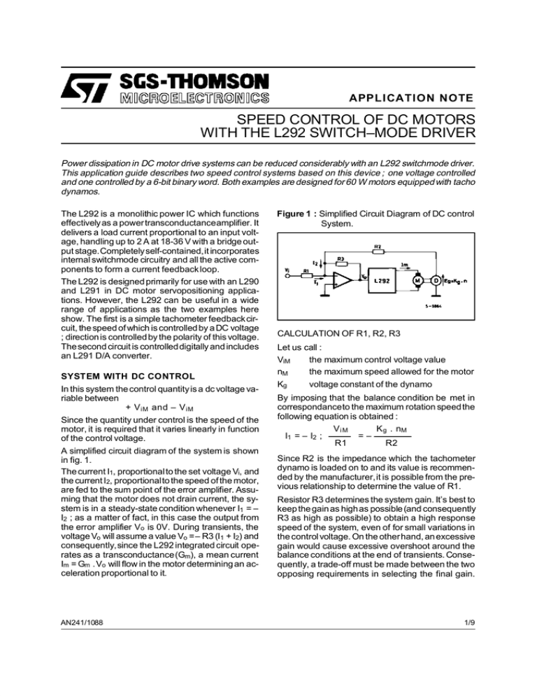
A simplified circuit diagram of the system is shown
in fig. 1.
The current I1, proportionalto the set voltage Vi, and
the current I2, proportionalto the speed of the motor,
are fed to the sum point of the error amplifier. Assuming that the motor does not drain current, the system is in a steady-state condition whenever I1 = –
I2 ; as a matter of fact, in this case the output from
the error amplifier Vo is 0V. During transients, the
voltage Vo will assume a value Vo =– R3 (I1 + I2) and
consequently,since the L292 integrated circuit operates as a transconductance(Gm), a mean current
Im = Gm . Vo will flow in the motor determining an acceleration proportional to it.
AN241/1088
Figure 1 : Simplified Circuit Diagram of DC control
System.
CALCULATION OF R1, R2, R3
Let us call :
the maximum control voltage value
ViM
nM
the maximum speed allowed for the motor
Kg
voltage constant of the dynamo
By imposing that the balance condition be met in
correspondanceto the maximum rotation speedthe
following equation is obtained :
K g . nM
Vi M
I1 = – I2 ;
=–
R1
R2
Since R2 is the impedance which the tachometer
dynamo is loaded on to and its value is recommended by the manufacturer,it is possible from the previous relationship to determine the value of R1.
Resistor R3 determines the system gain. It’s best to
keep the gain as highas possible (and consequently
R3 as high as possible) to obtain a high response
speed of the system, even of for small variations in
the control voltage. On the otherhand, an excessive
gain would cause excessive overshoot around the
balance conditions at the end of transients. Consequently, a trade-off must be made between the two
opposing requirements in selecting the final gain.
1/9
APPLICATION NOTE
The value for R3 should be theoretically determined
by studying the transfer function, by knowing the
electrical and mechanical constants of the motor as
well as the load applied to it.
A complete diagram of the circuit actually realized is
shown in fig. 2, while fig. 3, shows the characteristic
n = f (Vi) obtained.
Resistor R2 drawn in the simplified circuit diagram
has been split here in two parts and, in addition, a
capacitor has been interposed to ground to filter the
signal coming from the tachometer dynamo.
The curve n. 1 in fig. 3 refers to the operation of the
motor in no-load condition, with a current drain of
200 mA ; the curve n. 2 refers to a motor loaded so
as to drain a current of 1A. By disregarding the discontinuity around the origin, it can be notedthat the
characteristics are linear over the whole control voltage range.
By analyzing the curves around the origin, it can be
noted that the motor stands still as long as the input
signal does not exceed a certain threshold level,
which is as much higher as the current drained by
the motor is higher.
Let us call Gm the transconductanceof L292, and I
the starting current of the motor ; the voltage which
must be available at the input of L292 in order that
the motor starts turning is :
I
mA
Vo =
with Gm = 220
(typical value)
V
Gm
The corresponding control voltage will be :
R1
I
R1
=
.
.
Vi = Vo
R3
Gm
R3
and it is as much lower as the gain of the error amplifier is higher.
The presence of a control voltage interval in which
the motor stands still, can be useful when it is required that, for a certain position of potentiometer P1
(see fig. 2), the motor speed be zero. An other method to hold the motor still is to use the inhibits of
L292, for instance by grounding pin 13.
Figure 2 : Complete Circuit Diagram.
D1 ÷ D 4
2/9
{
VF ≤ 1.2 V @ I = 2 A
trr ≤ 200 ns
APPLICATION NOTE
It can be noted from fig. 3 that,by keepingthe control
voltage Vi constant, the speed varies according to
the motor current drain.
Let us call ∆I the current variation ; the voltage variation required at the input of L292 is
∆I
∆ Vo =
Gm
since the control voltageis constant, to generatethis
∆ Vo it is necessary that the rotation speed be varied
by a quantity ∆ n such as to have :
R3
∆I
=
∆
V
o =
.
.
Kg ∆ n
R2
Gm
∆n=
∆I
.
R2
Gm Kg
R3
(∆ I shall be taken with its sign)
Figure 3 : Output Characteristics of the Circuit in
fig. 2.
In this case too, the variation ∆ n is as much lower
as the error amplifier gain is higher. With the circuit
shownin fig. 2 ∆n isapproximately30 turns/min. with
∆ I = 800 mA, ∆n = 0.037 turns/mA.min approx.
It is possible to adopt a circuit which prevents the variation in the numberof turns in functionof motor current. The problem is to ”sense” the current flowing
throughthe motor and to senda current proportional
to it to the sum point of the error amplifier. The complete circuit which includes, beside the voltage feedback loop, also a current feed-back loop, is
illustrated in fig. 4.
In the integrated circuit L292, a current proportional
to the mean current drained by the motor flows between pin 5 and pin 7.
An operational amplifier amplifies the voltage drop
provokedby this current across a 510Ω resistor and
sends a current to the sum point which is consequently proportional to the mean current in the motor, the value of which can be made vary by acting
on potentiometer P2. By properly adjusting P2, a
condition can be achieved in which the speed does
not change when the current drained by the motor
varies.
The discontinuity around the origin, which was present in the previous circuit (fig. 2), is practically negligible in the circuit shown in fig. 4.
The characteristic n = f (Vi) relevant to the circuit of
fig. 4 is shown in fig. 5, and this characteristic does
not substantially change over the whole range of
currents allowed by the L292 (up to 2A).
In the circuit described above if the motor stall condition is requested. It is preferable to act on the inhibits of the integrated circuit L292, for instance by
groundingpin 13, instead of adjusting potentiometer
P1 : as a matter of fact, the exact position of this potentiometer is difficult to obtain, since the characteristic crosses the axis Vi in one only point (this
mean that n is only 0 for a very narrow interval of Vi).
3/9
APPLICATION NOTE
Figure 4 : Complete Circuit with Current Feedback.
D1 ÷ D 4
Figure 5 : Output Characteristics of the Circuit in
fig. 4.
{
V F ≤ 1.2 V @ I = 2 A
vement shall the clockwise or counter-clockwise.
For the circuit implementation, the integrated circuits L291 (which includes a D/A converter and two
operational amplifiers) and L292 are used.
A simplified circuit diagram is shown in fig. 6.
Figure 6 : Simplified Circuit Diagram (digital
control).
SYSTEM WITH DIGITAL CONTROL
In this system the speed information is given to the
circuit by a binary code made up of 5 information bits
plus one sign bit, which determines whether the mo4/9
APPLICATION NOTE
The current value I1 dependson the value of Iref and
on the value of inputs b1 through b5, where its sign
depends on the bs input.
The maximum value for I1, which is obtained whenever inputs b1 through b5 are low, is :
31
Vr ef
31
I1 max = Iref
=
.
16
R1
16
In order to have the system in a steady state condition (no current drained by the motor), it must be :
I1 = – I2
By imposing the balance condition at the maximum
speed, one obtains : I1 max = – I2 max
V r ef
31
K g nM
=
.
R1
16
R2
Figure 7 : Complete Circuit Diagram.
where
Kg = dynamo’s voltage constant
nM = maximum speed preset for the motor.
The current Iref, and consequently the ratio Vref/R1,
must lie within a certain range imposed by the D/A
converter actually used.
In our case, this range is 0.3 to 1 mA. The values of
R1 and R2 can be determined from the previous relationship.The same considerations made in the description of the DC control system apply for the
selection of R3.
A complete diagram of the circuit implemented is indicated in fig. 7, while the input versus output characteristics is shown in fig. 8.
D1 ÷ D 4
{
V F ≤ 1.2 V @ I = 2 A
5/9
APPLICATION NOTE
In the graph of fig. 8 the rotation speed of the motor
is represented on ordinates, while the decimal speed code, corresponding to the binary code applied
to inputs b1 throughb5, is representedon abscissae.
The abscissa 1 corresponds to the minimum speed
code,i.e. input b1 low and remaining inputshigh, since the least significant input is b1 andthe active status of inputs is low. The abscissa 31 corresponds to
the maximum speed code, i.e. all inputs b1 through
b5 low. The negative abscissae have been obtained
by changing the status of the bs input. The graph in
fig. 8 shouldhave beenmade up of a number of dots
; these dots have been joined together with an ininterrupted line for convenience. This graph has the
same features as the graph in fig. 3, i.e. the curve
features a discontinuity around the origin, and it lowers as long as the motor current drain increases.
In this case too, the circuit in fig. 7 can be modified
in order to prevent that the speed vary in function of
the motor load, by adding a current loop in the control circuit, by using the remaining operational amplifier available in the integrated circuit L291.
Since this amplifier has only the inverting input available, while the non-inverting input is grounded, a
Figure 8 : Output Characteristic of the Circuit in
fig. 7.
6/9
circuit arrangement as schematically shown in fig. 9
has been adopted in order to have an output signal
referred to ground, given an input signal referred to
a reference voltage (in L292) of approximately 8 V.
Figure 9 : Translator Circuit.
Resistors RA and RB must be high-precision resistors in order to have output 0 with no Im current present. In the practical implementation, resitors with
an accuracy of 5 % are used and the ends of a potentiometer are interposed between resitors RB and
the output to the sum point of the error amplifier is
made through the cursor. The gain of this current
loop is propotionalto the ratio R3/RB. Acomplete circuit diagram is shown in fig. 10.
Since, for reasonsof gain, resistor RB must be 27 kΩ
and, if connected to pin 7 of L292, should have subtracted too much current by thus affecting the correct operation of L292, it has been connected to
pin 11, having the same potential as pin 7. Consequently, the resistance value between pin 11 and
ground has been modified, in order to maintain the
switching frequency of L292 unchanged.In order to
have a correct adjustment of potentiometer P1, it is
enough to set the 0 speed code (b1 through b5 high)
and turn the cursor until the motor stops.
The input versus output characteristic obtained with
the circuit of fig. 10 is indicated in fig. 11.
APPLICATION NOTE
Figure 10 : Complete Circuit with Current Feedback.
D1 ÷ D4
Figure 11 : Output Characteristic of the Circuit in
fig. 10.
{
V F ≤ 1.2 V @ I = 2 A
RESPONSE TO INPUT STEP
Measurements have been taken on the circuits described in the previous paragraphs, in order to analyze how the motor speed varies when a step
variation is imposed to the input.
For the system DC control, the control voltage has
been changed from 0 to the maximum value ViM and
down to 0 again. For the digital system the speed
code has been changed from 0 (b1 through b5 high)
to the maximum value (b1 throughb5 low) and down
to 0 again. When the control quantity changes from
0 to the maximum value, the output voltage of the
error amplifier (Vo, fig. 1 and fig. 6) assumes its maximum value, since the feed-back signal coming
from the tachometer dynamoinitially 0. In theseconditions, L292 supplies the motor with the maximum
current (2A) and maintains it until the motor speed
is sufficiently close to the maximum value.
Since the motor is powered from a constant current,
it moves with a constant current, it moves with a constant acceleration and consequently its speed
grows linearly from 0 up to the maximum value over
the time interval ta. The time needed for the motor
to reach the maximum speed also depends,besides
7/9
APPLICATION NOTE
the current, on the electrical and mechanical characteristics of the motor and on the moment of inertial
of the load applied to the motor. When the control
quantity changes from the maximum value to 0, the
output of the error amplifier Vo assumes the maximum value, but with an opposite sign with respect
to the previous case, and the current flowing in the
motor is also reversed and tends to brake it, by making the speed linearly decrease from the maximum
value down to 0 over the time period tf. The no-load
characteristics, relevant to the motor used for the
previous tests, are shown in fig. 12. The times ta and
tf are not equal to each other, which circumstance
is basically due to the frictions which, during the acceleration phase, oppose increase of speed, while
during the deceleration phase they contribute to
make the speed decrease. As a matter of fact, from
the movement equation :
.
..
J Θ + D Θ + T f = KT I M
where :
J=
System moment of inertia
D=
Coefficient of viscous friction
Tf =
Braking couple
Kt =
Motor constant
.
Θ=
Angular speed
..
Θ=
Angular acceleration
..
and by disregarding the term DΘ, one obtains:
.. KT ⋅ IM ± Tf
Θ=
J
..
where from it can be seen that | Θ | is greater if IM
is negative.
8/9
Figure 12 : Pulse Response.
APPLICATION NOTE
Information furnished is believed to be accurate and reliable. However, SGS-THOMSON Microelectronics assumes no responsibility for
the consequences of use of such information nor for any infringement of patents or other rights of third parties which may result from its
use. No license is granted by implication or otherwise under any patent or patent rights of SGS-THOMSON Microelectronics. Specifications mentioned in this publication are subject to change without notice. This publication supersedes and replaces all information previously supplied. SGS-THO MSON Microelectronics products are not authorized for use as critical components in life support devices or
systems without express written approval of SGS-THOMSON Microelectronics.
1995 SGS-THOMSON Microelectronics - All Rights Reserved
SGS-THOMSON Microelectronics GROUP OF COMPANIES
Australia - Brazil - France - Germany - Hong Kong - Italy - Japan - Korea - Malaysia - Malta - Morocco - The Netherlands - Singapore Spain - Sweden - Switzerland - Taiwan - Thaliand - United Kingdom - U.S.A.
9/9


