TEP
5.1.13
-00
Electron diffraction
Related Topics
Bragg reflection, Debye-Scherrer method, lattice planes, graphite structure, material waves, de Broglie
equation.
Principle
This famous experiment demonstrates the wave-particle duality of matter using the example of electrons.
The diffraction pattern of fast electrons passing a polycrystalline layer of graphite is visualized on a fluorescent screen. The interplanar spacing in graphite is determined from the diameter of the rings and the
accelerating voltage. For the investigations on this phenomenon Louis de Broglie won the Nobel Prize in
1929 and George Thomson and Clinton Davisson in 1937.
Equipment
1
1
1
1
1
1
2
2
2
1
1
2
Electron diffr. tube a. mounting
High voltage supply unit, 0-10 kV
Connecting cord, 30 kV, 500 mm
Power supply, 0...600 VDC
Vernier caliper, plastic
Connecting cord, l = 750 mm, green-yellow
Connecting cord, l = 250 mm, green-yellow
Connecting cord, l = 100 mm, yellow
Connecting cord, l = 750 mm, red
Connecting cord, l = 750 mm, yellow
Connecting cord, l = 750 mm, blue
Connecting cord, l = 750 mm, black
06721.00
13670.93
07366.00
13672.93
03014.00
07362-15
07360-15
07359-02
07362.01
07362.02
07362.04
07362.05
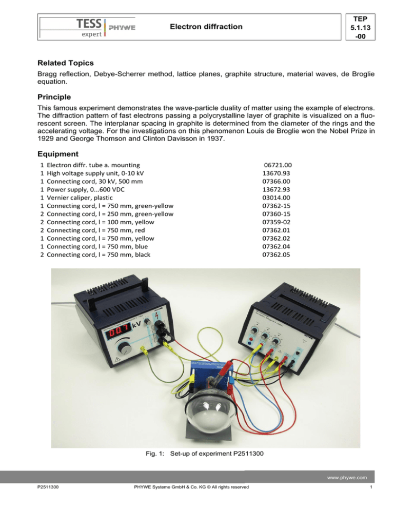
Fig. 1: Set-up of experiment P2511300
www.phywe.com
P2511300
PHYWE Systeme GmbH & Co. KG © All rights reserved
1
TEP
5.1.1300
Electron diffraction
Tasks
1. Measure the diameter of the two smallest diffraction rings at different anode voltages.
2. Calculate the wavelength of the electrons from the anode voltages.
3. Determine the interplanar spacing of graphite from the relationship between the radius of the diffraction rings and the wavelength.
Set-up and Procedure
Set up the experiment as shown in Fig. 1. Connect the sockets of the electron diffraction tube to the
power supply as shown in Figs. 1 and 2.
Fig. 2: Electrical connections for the experiment.
Set the Wehnelt voltage G1 and the voltages at grid 4
(G4) and G3 so that sharp, welldefined diffraction rings
appear. Read the anode voltage at the display of the HV
power supply. To determine the diameter of the diffraction rings, measure the inner and outer edge of the rings
with the vernier caliper (in a darkened room) and take
an average. Note that there is another faint ring immediately behind the second ring.
Theory and evaluation
In 1926, De Broglie predicted in his famous hypothesis
that particles should also behave like waves. This hypothesis was confirmed concerning electrons three years
later independently by George Thomson and Clinton Fig. 3: Set-up and power supply to the electron diffracDavisson, who observed diffraction patterns of a beam tion tube.
2
PHYWE Systeme GmbH & Co. KG © All rights reserved
P2511300
TEP
5.1.13
-00
Electron diffraction
of electrons passing a metal film and a crystalline grid, respectively. All of them won the Nobel prize for
their investigations, De Broglie in 1929 and Thomson and Davisson in 1937.
Electron diffraction is used to investigate the crystal structure of solids similar to X-Ray diffraction. Crystals contain periodic structural elements serving as a diffraction grating that scatters the electrons in a
predictable way. Thus, the diffraction pattern of an electron beam passing through a layer of a crystalline
material contains information about the respective crystal structure. In contrast to X-Rays, electrons are
charged particles and therefore interact with matter through coulomb forces providing other information
about the structure than X-ray diffraction.
To explain the interference phenomenon of this experiment, a wavelength λ, which depends on momentum, is assigned to the electrons in accordance with the de Broglie equation:
(1)
where h = 6.625 · 10–34 Js, Planck’s constant.
The momentum can be calculated from the velocity ν that the electrons acquire under acceleration voltage UA:
(2)
The wavelength is thus
(3)
where e = 1.602 · 10–19 As (the electron charge)
and m = 9.109 · 10–31 kg (rest mass of electron).
At the voltages UA used, the relativistic mass can
be replaced by the rest mass with an error of only
0.5%. The electron beam strikes a polycrystalline
graphite film deposite on a copper grating and is
reflected in accordance with the Bragg condition:
(4)
where d is the spacing between the planes of the
carbon atoms and θ is the Bragg angle (angle between electron beam and lattice planes).
In polycrystalline graphite the bond between the individual layers (Fig. 4) is broken so that their orientation is random. The electron beam is therefore
spread out in the form of a cone and produces interference rings on the fluorescent screen. The Fig. 4: Crystal lattice of graphite.
Bragg angle θ can be calculated from the radius of
www.phywe.com
P2511300
PHYWE Systeme GmbH & Co. KG © All rights reserved
3
TEP
5.1.1300
Electron diffraction
the interference ring but it should be remembered
that the angle of deviation α (Fig. 3) is twice as
great:
α = 20.
From Fig. 3 we read off
(5)
where R = 65 mm, radius of the glass bulb.
Fig. 5 : Graphite planes for the first two interference
rings.
α
Now,
For small angles α (cos 10° = 0.985) can put
α
(6)
so that for small angles θ we obtain
θ
θ (6a)
With this approximation we obtain
(7)
The two inner interference rings occur through reflection
from the lattice planes of spacing d1 and d2 (Fig. 5), for
n = 1 in (7).
The wavelength is calculated from the anode voltage in
accordance with (3):
4.00
4.50
5.00
5.50
6.50
7.00
7.40
4
19.4
18.3
17.3
16.5
15.2
14.7
14.3
Fig. 6: Radii of the first two interference rings as a function of the wavelength of the electrons.
PHYWE Systeme GmbH & Co. KG © All rights reserved
P2511300
Electron diffraction
TEP
5.1.13
-00
Applying the regression lines expressed by
Y = AX + B
to the measured values from Fig. 6 gives a slopes
A1 = 0.62 (2) · 109
A2 = 1.03 (2) · 109
and the lattice constants
d1 = 211 pm
d2 = 126 pm
in accordance with (7),
Fig. 7: Interplanar spacing in graphite
d1 = 213 pm; d2 = 123 pm; d3 = 80.5 pm;
d4 = 59.1 pm; d5 = 46.5 pm.
and
Notes
-
The intensity of higher order interference rings is much lower than that of first order rings. Thus, for
example, the second order ring of d1 is difficult to identify and the expected fourth order ring of d1
simply cannot be seen. The third order ring of d1 is easy to see because graphite always has two lattice planes together, spaced apart by a distance of d1/3. (Fig. 7) In the sixth ring, the first order of ring
of d4 clearly coincides with the second order one of d2.
Radii (mm) calculated according to (4) for the interference rings to be expected when UA = 7 kV:
-
-
n=1
n=2
n =3
n=4
d1
8.9
17.7
26.1
34.1
d2
15.4
29.9
d3
23.2
d4
31.0
d5
38.5
The visibility of high order rings depends on the light intensity in the laboratory and the contrast of the
ring system which can be influenced by the voltages applied to G1 and G4.
The bright spot just in the center of the screen can damage the fluorescent layer of the tube. To avoid
this reduce the light intensity after each reading as soon as possible.
www.phywe.com
P2511300
PHYWE Systeme GmbH & Co. KG © All rights reserved
5
