Interfacial charge behavior in nanodielectrics
advertisement
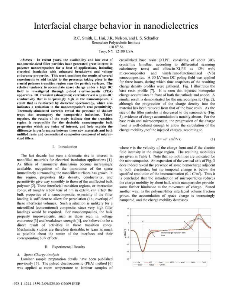
Interfacial charge behavior in nanodielectrics R.C. Smith, L. Hui, J.K. Nelson, and L.S. Schadler Rensselaer Polytechnic Institute 110 8th St. Troy, NY 12180 USA Abstract - In recent years, the availability and low cost of nanometric-sized filler particles have generated great interest in polymer nanocomposites for a host of applications, including electrical insulation with enhanced breakdown and voltage endurance properties. This work combines the results of several experiments to add insight to the processes taking place in the crucial polymer transition region near the particle surfaces. The relative tendency to accumulate space charge under a high DC field is investigated through pulsed electroacoustic (PEA) apparatus. DC transient (absorption) currents reveal a quasi-DC conductivity that is surprisingly high in the nanocomposite, a result that is reinforced by dielectric spectroscopy, which also indicates a reduction in the nanocomposite’s real permittivity. Thermally-stimulated currents reveal the presence of shallow traps that accompany the nanoparticle inclusions. Taken together, the results of the study indicate that the transition region is responsible for the desirable nanocomposite bulk properties which are today of interest, and help explain the difference in performance between these new materials and both unfilled resin and conventional composites composed of micronsized fillers. crosslinked base resin (XLPE, consisting of about 30% crystalline lamellae, according to differential scanning calorimetry tests) and silica-in-XLPE as 12½ wt% microcomposites and vinylsilane-functionalized (VS) nanocomposites. A 30 kV/mm DC poling field was applied for three hours, during which time snapshots of the resulting charge density profiles were gathered. Fig. 1 illustrates the base resin profile [7]. It is seen that injected homopolar charge accumulates in front of both the cathode and anode. A similar result is demonstrated for the microcomposite (Fig. 2), although the progression of the charge density into the material has been reduced from that of the base resin. As the size of the filler particles is decreased to the nanometric (Fig. 3), evidence of charge accumulation is notably absent. For the base resin and microcomposite, the progression of the charge front is well-defined enough to allow the calculation of the charge mobility μ of the injected charges, according to I. Introduction where v is the velocity of the charge front and E the electric field intensity in the charge region. The resulting mobilities are given in Table 1. Note that no mobilities are indicated for the nanocomposite. An expansion of the vertical axis of Fig. 3 does indeed reveal the presence of some homocharge adjacent to both electrodes, but its temporal change is below the specified resolution of the instrumentation (0.1 C/m3). Thus it is concluded that the introduction of microparticles reduces the charge mobility by about half, while nanoparticles provide some further hindrance to the movement of charge. Stated another way, as the polymer/filler interfacial volume fraction grows, the accumulation of space charge is increasingly hampered, and the charge mobility decreases. The last decade has seen a dramatic rise in interest in nanofilled materials for electrical insulation applications [1]. As fillers of nanometric dimensions become increasingly available, recognition of the importance of the space immediately surrounding the nanofiller surfaces has grown. In this region, properties like density, conductivity, and permittivity give way smoothly to those of the unaffected bulk polymer [2]. These interfacial transition regions, or interaction zones, of roughly a few tens of nm in extent, can affect the bulk properties of a nanocomposite, especially if the filler loading is sufficient to allow for percolation (i.e., overlap) of these interfacial volumes. Such a situation is unlikely for a microfilled (conventional) composite, since very high filler loadings would be required. For nanocomposites, the bulk property improvements, such as those seen in voltage endurance [3] and breakdown strength [4], are believed to be a direct result of activities in these transition zones. Mechanistic studies are therefore desirable, to learn as much as possible about the nature of the interfaces and their corresponding bulk effects. II. Experimental Results A. Space Charge Analysis Laminar sample preparation details have been published previously [5]. The pulsed electroacoustic (PEA) method [6] was applied at room temperature to laminar samples of 978-1-4244-4559-2/09/$25.00 ©2009 IEEE μ = v/E (m2/Vs) (1) Fig. 1. PEA charge density profile for base XLPE [7]. The sample was poled at 30 kV/mm DC for 3½ hours at room temperature. Times are in seconds. Fig. 2. PEA charge density profile for 12½ wt% microcomposite [7]. Fig. 3. PEA charge density profile for 12½ wt% VS-nanocomposite [7]. TABLE I Charge mobilities from the room-temperature PEA experiment (10-17 m2/Vs). No nanocomposite mobility is indicated since no movement of the charge fronts was detected. Material XLPE Micro VS-Nano Cathode 14 4.1 -- Anode 16 7.1 -- Absorption Current Room-temperature absorption currents were measured by applying 30 kV/mm DC to the laminar samples and measuring the resulting currents as a function of time. Absorption current measurements are sometimes used to investigate the presence of polarization, space charge accumulation, slow dipole orientation, and quasi-DC conduction [8]. Fig. 4 illustrates the results of the experiment. The microcomposite displays a curious current rise, beginning at about 900 seconds, which continues throughout the testing duration. In fact, conventional composite materials used for electrical insulator applications are known to experience MaxwellWagner-Sillars polarization at the matrix/filler interfaces [9], which is characterized by a slow migration of charges with accumulation at these interfaces. Another interesting feature of the absorption plot is the quasi-DC (10,000 second) conductivity that is calculated from the measured currents (all test samples had nominally identical geometry). The nanocomposites, both untreated and VS-functionalized, appear to be approaching higher values of conductivity (4.8 and 3.4x10⁻¹⁶ S/m, respectively), while the base resin’s 10,000 second value is 1.4x10⁻¹⁶ S/m. This is a surprising result, since the conductivity of the silica filler is approximately an order of magnitude below that of polyethylene. 6 hour conductivity experiment results at 60oC (not shown) confirm this general result: the nanocomposites are more conductive than the base resin, at least at 12½ wt% (5½ vol%) loading. C. Dielectric Spectroscopy Low-field, room-temperature spectroscopy was performed on laminar samples of base resin and 12½ wt% composites. Fig. 5 presents the real permittivity spectra for frequencies 10-4 Hz < f < 106 Hz. Over the entire frequency range, the nanocomposites display permittivities lower than those of the microcomposite, even though the filler volume fractions are the same. Good permittivity predictions have previously been demonstrated for conventional composites using established composite mixing laws (e.g., Landau-Lifschitz and MaxwellGarnett [10]), but nanocomposites often do not comply well with these relationships. In fact, nanocomposite permittivities in some frequency ranges have been found to be less than those of each of their constituents [3,5]. This suggests that the pervasive interaction zone in the nanocomposite plays a notable role in the dielectric behavior, since the possibility of entangled polymer chains and bonding or other interactions with the filler can reduce the dipole-moment density [2]. Further, the nanocomposites do not show evidence of lowfrequency interfacial polarization to the same extent as the microcomposite. Fig. 6 gives the imaginary (loss) permittivity spectra. The nanocomposites and microcomposite show a simultaneous increase of their real (Fig. 5) and imaginary permittivities as low frequencies are approached; the subsequent buildup of charge results in an apparent rise in the real permittivity. However, the nanocomposites’ real, lowfrequency permittivities are not as high, B. Fig. 4. 30 kV/mm, room-temperature absorption currents for unfilled XLPE and 12½ wt% composites [7]. suggesting that the contribution made by quasi-DC conduction is greater in the nanocomposites than for the microcomposite. If percolation of the interaction regions is assumed [11], the increased nanocomposite quasi-DC conductivity is likely a result of increased conductivity in the transition region. It has been suggested that the space surrounding nanometric fillers tends to be quite heavily charged [2], the result of migration of compensating charges during the molding process. Again, with percolation assumed, the higher conductivity of this charge layer would mitigate the MWS buildup of charges by providing a complete conduction path through the bulk. This also could explain the increase in quasi-DC conductivity (with respect to the base XLPE) that was seen in the absorption experiment (Fig. 4). D. Thermally-Stimulated Current An investigation was conducted into the depths of carrier traps that exist in the base resin and composites. For that purpose, a thermally-stimulated current (TSC) experiment [12] was carried out on the materials, using laminar samples that were heated to 80oC, then cooled to -100oC under liquid nitrogen while being poled at 30 kV/mm. The poling field was then removed, and each sample heated at 3oC per minute to +100oC while being shorted through a recording picoammeter. The resulting current peaks, as a function of the absolute temperature T, are fitted to Arrhenius plots to determine the trap depths Et according to I = Iδ exp[-Et/kT] (2) where Iδ is a constant and k is the Boltzmann constant. Fig. 7 illustrates an example of the TSC results for 12½ wt% VSnanocomposite. The location of the 63oC peak is slightly elevated from that of unfilled XLPE (60oC), presumably due to the bonding of polymer chains to the particles through the coupling agent [13]. The sources of the traps (crystalline defects, crystalline/amorphous interfaces, etc.) have been determined through prior experimentation [14]. More importantly, an examination of the deepest traps in each of the materials tested (Table II) reveals that all the nanocomposites possess a population of traps that are considerably shallower than the unfilled and microfilled resins. This could have important implications for the transport of charge throughout the bulk of the nanocomposites, since thermal promotion of charges to the conduction band depends upon the minimum energy required Ec-Et, where Ec is the energy at the bottom of the conduction band [15]. Therefore, a significant number of shallower traps could explain the larger quasi-DC conduction Fig. 5. Real relative permittivity ε’ for base resin and 12½ wt% composites at room temperature [11]. Fig. 7. Thermally-stimulated current for 12½ wt% VS-nanocomposite, poled at 30 kV/mm and 80oC [7]. The defect sources were taken from TSC literature [14]. TABLE 2 Trap depths from the thermally-stimulated current experiment. The traps indicated are the deepest from each material. No discernible traps were detected for the 25 and 30 wt% VS-nanocomposite, possibly indicative of percolative conduction without trapping. Material Fig. 6. Imaginary relative permittivity ε” for base resin and 12½ wt% composites at room temperature [11]. XLPE 12½% Micro 12½% VS-Nano 20% VS-Nano 25% VS-Nano 30% VS-Nano Deepest Traps (eV) 0.46 0.83 0.14 0.07 --- currents detected in the absorption and 6-hour conductivity tests. At higher loadings, evidence of trapping disappears altogether, possibly reflecting the thorough percolation of the interaction zones between particles and agglomerates. At these high loadings, it is possible that the conductivity is so high that deep traps are simply bypassed altogether as conduction charges move between the shallower ones. region or other mechanisms are more relevant for explaining the improved breakdown strength. For example, recent work suggests that mitigation of voids and other low-permittivity inclusions, along with a possible charge scattering mechanism by the interfacial ionic charge layers, could play a critical role in breakdown strength improvements [11]. REFERENCES III. Discussion and Conclusions The PEA space charge density test presents an apparent contradiction to the absorption and dielectric spectroscopy results, in that the latter two tests indicate relatively high lowfrequency conductivity for the nanocomposites, while it is reasoned from the PEA results that the VS-nanocomposite has very low charge mobility. Further, it was presumed that this low mobility was the reason that very little space charge had accumulated. At the same time, TSC results on base resin, the microcomposite, and various loadings of nanocomposites show that, by comparison, the nanocomposites’ trap sites are shallower than those of the other materials. It has been previously hypothesized that a significant distribution of shallower (i.e., higher-energy) traps can provide distinct and separate conduction pathways through the bulk of a polymer [16], raising the conductivity while simultaneously decreasing the capture of space charge as it bypasses deep traps in favor of shallower ones. Such behavior matches that seen in the present work. Prior research using electron paramagnetic resonance (EPR) [13] has indicated that the silica nanoparticles introduce oxygen radicals which have also been shown to participate in conduction [17]. With all the test results considered, the following summarizes the nanoscale characteristics in the transition region surrounding the filler particles. Particle-polymer interactions reduce the chain mobility near the particle surfaces, causing a reduction in the bulk real permittivity when compared to conventional composites, and even unfilled resins. At the same time, an interfacial charge layer provides donor/acceptor carrier sites for increased conductivity in the bulk polymer. This may explain a relative lack of space charge buildup as well, where deeper traps are “short circuited” by the presence of the shallower ones; charge movement involving deep traps is reduced, resulting in a lower deep-trap charge mobility in the PEA experiment. The mechanistic testing of this work was conducted at low to medium electric field intensities, and thus it is not clear how this new understanding of the transition region translates into improved breakdown strength, since the breakdown avalanche of charges occurs at much higher fields. The increased bulk conductivity brought about by the percolated interaction zones seems to suggest that the breakdown strengths should be lowered for the nanocomposites, which is not the case [11]. Moreover, the conductivity increase, a product of the shallow trap distribution introduced by the nanoparticles, actually decreases the amount of electrode-shielding homocharge (Fig. 3), which should also tend to decrease the breakdown strength. This suggests, therefore, that other properties of the transition [1] L.A. Dissado and J.C. Fothergill, “Dielectrics and Nanotechnology,” IEEE Trans. Diel. Elec. Ins., Vol. 11, No. 5, pp. 737-738, Oct. 2004. [2] T.J. Lewis, “Interfaces are the Dominant Feature of Dielectrics at the Nanometric Level,” IEEE Trans. Diel. Elec. Ins., Vol. 11, No. 5, pp. 739-753, Oct. 2004. [3] J.K. Nelson and Y. Hu, “The Impact of Nanocomposite Formulations on Electrical Voltage Endurance,” Proc. Int. Conf. Solid Diel., Toulouse, France, July 2004. [4] M. Roy, J.K. Nelson, R.K. MacCrone, and L.S. Schadler, “Candidate mechanisms controlling the electrical characteristics of silica/XLPE nanodielectrics,” J. Mat. Sci., Vol. 42, pp. 3789-3799, Feb. 2007 [5] R.C. Smith, C. Liang, M. Landry, J.K. Nelson, and L.S. Schadler, “Studies to unravel some underlying mechanisms in nanodielectrics,” Proc. Conf. Elec. Ins. Diel. Phen., pp. 286-289, Oct. 2007. [6] O. Gallot-Lavallée and G. Teyssedre, “Space charge measurements in solid dielectrics by the pulsed electro-acoustic technique,” Proc. Int. Conf. Solid Diel., Toulouse, France, July 2004. [7] Formulation and Characterization of Nanocomposite Insulation for Utility Cable Application, Electric Power Research Institute report, Dec. 2008. [8] D.K. Das-Gupta, “Conduction Mechanisms and High-field Effects in Synthetic Polymers,” IEEE Trans. Diel. Elec. Ins., Vol. 4, No. 2, pp. 149-156, Apr. 1997. [9] Y. Zhu, K.S. Suh, and H. Xie, “Interfacial Effect on Electrical Conductivity in Filled Polymer Composite,” Proc. Int. Conf. Props. and Appls. Diel. Matls., Seoul, S. Korea, pp. 918-921, May 1997. [10] A.H. Sihvola and E. Alanen, “Studies of Mixing Formulae in the Complex Plane,” IEEE Trans. Geosci. Remote Sens., Vol. 29, No. 4, pp. 679-687, July 1991. [11] R.C. Smith, Mechanistic Electrical Behavior of Crosslinked Polyethylene/Silica Nanocomposites, PhD thesis, Rensselaer Polytechnic Institute, May 2009. [12] K.S. Suh, J. Tanaka, and D. Damon, “What is TSC,” IEEE Elec. Ins. Mag., Vol. 8, No. 6, pp. 13-20, Nov. 1992. [13] M. Roy, An Examination of the Potential for Nano-Composites in the Formulation of HV Cable Insulation, Ph.D. thesis, Rensselaer Polytechnic Institute, 2005. [14] M. Ieda, “Recent Topics of High Field Phenomena in Insulating Polymers,” Proc. Int. Conf. Prop. Apps. Diel. Matls, pp. 35-38, July 1994. [15] M.A. Lampert and P. Mark, Current Injection in Solids, New York: Academic Press, pp. 3-43, 1970. [16] G.C. Montanari, D. Fabiani, F. Palmieri, D. Kaempfer, R. Thomann, and R. Mulhaupt, “Modification of Electrical Properties and Performance of EVA and PP Insulation through Nanostructure by Organophilic Silicates,” IEEE Trans. Diel. Elec. Ins., Vol. 11, No. 5, pp. 754-762, Oct. 2004 [17] R.K. MacCrone, J.K Nelson, R.C. Smith, and L.S. Schadler, “The use of paramagnetic resonance in the probing of the nano-dielectric interface,” IEEE Trans. Diel. Elec. Ins., Vol. 15, No. 1, pp. 197-204, Feb. 2008. ACKNOWLEDGMENT The authors would like to thank the Electric Power Research Institute (EPRI) for supporting this work. Author address: Rob Smith, Rensselaer Polytechnic Inst., Troy, NY 12180-3590, USA Email: smithr8@rpi.edu
