USBULC6-2M6
Ultra large bandwidth ESD protection
Features
■
2 data line 15 kV ESD protection
■
Protects 5 V VBUS when applicable
■
Ultra low capacitance: 0.65 pF at F = 240 MHz
■
Very low leakage current: 0.5 µA max.
■
Fast response time compared with varistors
■
µQFN 6 lead package
■
RoHS compliant
Benefits
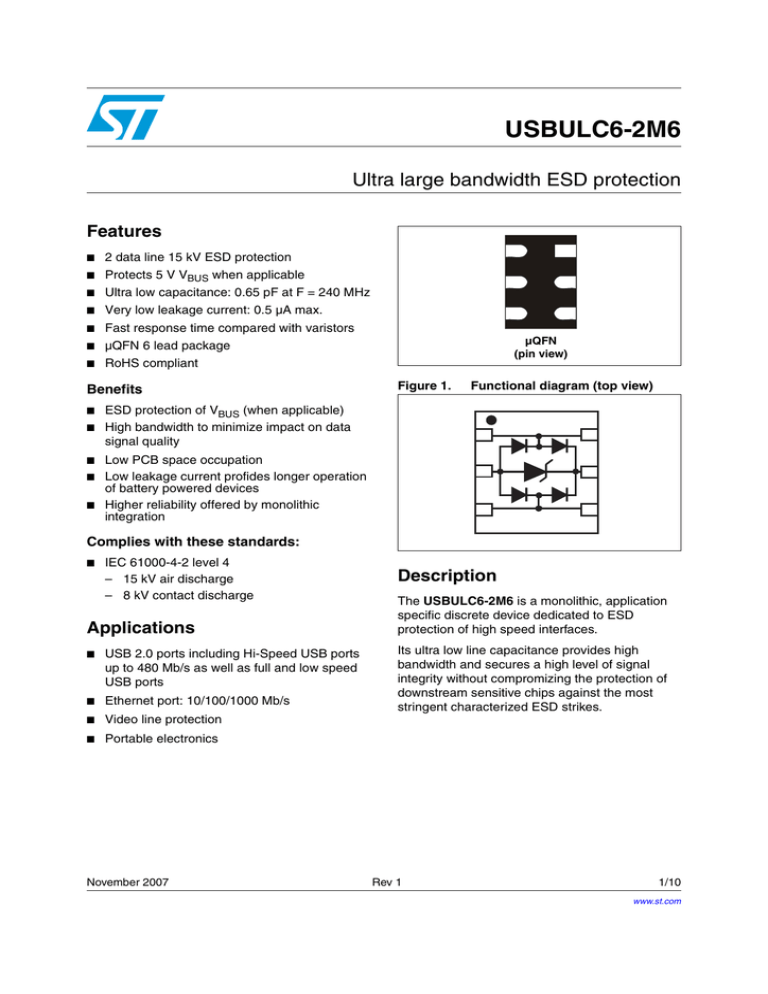
µQFN
(pin view)
Figure 1.
Functional diagram (top view)
■
ESD protection of VBUS (when applicable)
■ High bandwidth to minimize impact on data
signal quality
■
Low PCB space occupation
Low leakage current profides longer operation
of battery powered devices
■ Higher reliability offered by monolithic
integration
■
Complies with these standards:
■
IEC 61000-4-2 level 4
– 15 kV air discharge
– 8 kV contact discharge
Applications
■
USB 2.0 ports including Hi-Speed USB ports
up to 480 Mb/s as well as full and low speed
USB ports
■
Ethernet port: 10/100/1000 Mb/s
■
Video line protection
■
Portable electronics
November 2007
Description
The USBULC6-2M6 is a monolithic, application
specific discrete device dedicated to ESD
protection of high speed interfaces.
Its ultra low line capacitance provides high
bandwidth and secures a high level of signal
integrity without compromizing the protection of
downstream sensitive chips against the most
stringent characterized ESD strikes.
Rev 1
1/10
www.st.com
Characteristics
1
USBULC6-2M6
Characteristics
Table 1.
Absolute ratings
Symbol
Parameter
VPP
Peak pulse voltage
Tstg
Storage temperature range
Value
Unit
±15
±15
±25
kV
-55 to +150
°C
IEC 61000-4-2 air discharge
IEC 61000-4-2 contact discharge
MIL STD883G-Method 3015-7
Tj
Maximum junction temperature
150
°C
TL
Lead solder temperature (10 seconds duration)
260
°C
Table 2.
Electrical characteristics (Tamb = 25 °C)
Value
Symbol
Parameter
Test conditions
Unit
Min.
IRM
Leakage current
VRM = 5 V
VBR
Breakdown voltage between VBUS
and GND
IR = 1 mA
VCL
Ci/o-GND
ΔCi/o-GND
Ci/o-i/o
2/10
Typ.
Max
0.5
6
µA
V
IPP = 1 A, tp = 8/20 µs
Any I/O pin to GND
12
V
IPP = 5 A, tp = 8/20 µs
Any I/O pin to GND
17
V
Clamping voltage
VR = 0 V, F = 1 MHz
Any I/O pin to ground
0.95
1.1
VR = 0 V, F = 240 MHz
Any I/O pin to ground
0.65
0.85
VR = 0 V, F = 1 MHz
Any I/O pin to ground
0.020
VR = 0 V, F = 1 MHz
Ground not connected
0.5
0.55
VR = 0 V, F = 240 MHz
Ground not connected
0.35
0.4
Capacitance between I/O and GND
Capacitance variation between I/O
and GND
pF
Capacitance between I/O
USBULC6-2M6
Figure 2.
Characteristics
Line capacitance versus frequency Figure 3.
(typical values)
C(fF)
Relative variation of leakage
current versus junction
temperature (typical values)
IRM[Tj] / IRM[Tj=25°C]
1000.0
5
900.0
4
800.0
700.0
3
I/O - GND
600.0
500.0
400.0
2
I/O – I/O
300.0
200.0
100.0
F(GHz)
Tj(°C)
0.0
0
1
Figure 4.
2
3
Attenuation measurement
1
25
50
Figure 5.
75
100
125
Crosstalk measurements
dB
S21(db)
0.00
0.00
- 4.00
- 30.00
- 8.00
- 60.00
- 12.00
- 90.00
F(Hz)
F (Hz)
- 16.00
- 120.00
300.0k
Figure 6.
1.0M
3.0M
10.0M
30.0M
100.0M
300.0M
1.0G
3.0G
Remaing voltage on I/O1 after the
USBULC6-2M6 during positive
ESD surge (15 kV Air)
300.0k
Figure 7.
1.0M
3.0M
10.0M
30.0M
100.0M
300.0M
1.0G
3.0G
Remaing voltage on I/O2 after the
USBULC6-2M6 during negative
ESD surge (15 kV Air)
10V/Div
10V/Div
100ns/Div
100ns/Div
3/10
Characteristics
Figure 8.
USBULC6-2M6
Remaing voltage on VBUS after the
USBULC6-2M6 during positive
ESD surge (15 kV Air)
10V/Div
Figure 9.
Remaing voltage on VBUS after the
USBULC6-2M6 during negative
ESD surge (15 kV Air)
10V/Div
100ns/Div
100ns/Div
Figure 10. Eye diagram PCB only
400 mV amplitude, F = 480 Mbps
Figure 11. Eye diagram PCB + USBULC6-2M6
400 mV amplitude, F = 480 Mbps
Horiz: 350 ps/div
Vert: 100 mV/div
Horiz: 350 ps/div
Vert: 100 mV/div
Figure 12. Eye diagram PCB + USBULC6-2M6, +5 V on VBUS decoupling capacitor
100 nF, 400 mV amplitude, F = 480 Mbps
Horiz: 350 ps/div
Vert: 100 mV/div
4/10
USBULC6-2M6
2
Application example
Application example
Figure 13. One differential line
D+
I/O1
To GND
plane
I/O2
1
6
2
5
3
4
I/O1
100 nF
I/O2
D-
3
Ordering information scheme
Figure 14. Ordering information scheme
USB ULC 6 - 2 M6
Product Designation
Ultra low capacitance
Breakdown Voltage
6 = 6 Volts
Number of lines protected
2 = 2 lines
Package
µQFN - 6 leads
5/10
Package information
4
USBULC6-2M6
Package information
●
Epoxy meets UL94, V0
In order to meet environmental requirements, ST (also) offers these devices in ECOPACK®
packages. ECOPACK® packages are Lead-free. The category of second level Interconnect
is marked on the inner box label, in compliance with JEDEC Standard JESD97. The
maximum ratings related to soldering conditions are also marked on the inner box label.
ECOPACK is an ST trademark. ECOPACK specifications are available at: www.st.com.
Table 3.
Micro QFN 1.45x1.00 6L dimensions
Dimensions
D
Ref.
N
E
1
2
A
A1
1
Millimeters
Inches
Min.
Typ.
Max.
Min.
Typ.
A
0.50
0.55
0.60
0.020 0.022 0.024
A1
0.00
0.02
0.05
0.000 0.001 0.002
b
0.18
0.25
0.30
0.007 0.010 0.012
D(1)
1.45
0.057
L
E(1)
1.00
0.039
k
(2)
0.50
0.020
2
e
b
e
K
0.20
L
0.30
Max.
0.008
0.35
0.40
0.012 0.014 0.016
1. ± 0.1 mm
2. ± 0.05 mm
Note:
Product marking may be rotated by 90° for assembly plant differentiation. In no case should
this product marking be used to orient the component for its placement on a PCB. Only pin
1 mark is to be used for this purpose.
Figure 15. Footprint dimensions in mm [inches]
0.50
[0.020]
0.25
[0.010]
0.65
[0.026]
0.30
1.60
[0.012] [0.063]
6/10
USBULC6-2M6
Recommendation on PCB assembly
5
Recommendation on PCB assembly
5.1
Stencil opening design
1.
General recommendation on stencil opening design
a)
Stencil opening dimensions: L (Length), W (Width), T (Thickness)
Figure 16. Stencil opening dimensions.
L
T
b)
W
General Design Rule
Stencil thickness (T) = 75 ~ 125 µm
W
Aspect Ratio = ----- ≥ 1.5
T
L×W
Aspect Area = ---------------------------- ≥ 0.66
2T ( L + W )
2.
5.2
Reference design
a)
Stencil opening thickness: 100 µm
b)
Stencil opening for leads: Opening to footprint ratio is 90%.
Solder paste
1.
Halide-free flux qualification ROL0 according to ANSI/J-STD-004.
2.
“No clean” solder paste is recommended.
3.
Offers a high tack force to resist component movement during high speed
4.
Solder paste with fine particles: powder particle size is 20-45 µm.
7/10
Recommendation on PCB assembly
5.3
5.4
5.5
USBULC6-2M6
Placement
1.
Manual positioning is not recommended.
2.
It is recommended to use the lead recognition capabilities of the placement system, not
the outline centering
3.
Standard tolerance of ± 0.05 mm is recommended.
4.
3.5 N placement force is recommended. Too much placement force can lead to
squeezed out solder paste and cause solder joints to short. Too low placement force
can lead to insufficient contact between package and solder paste that could cause
open solder joints or badly centered packages.
5.
To improve the package placement accuracy, a bottom side optical control should be
performed with a high resolution tool.
6.
For assembly, a perfect supporting of the PCB (all the more on flexible PCB) is
recommended during solder paste printing, pick and place and reflow soldering by
using optimized tools.
PCB design preference
1.
To control the solder paste amount, the closed via is recommended instead of open
vias.
2.
The position of tracks and open vias in the solder area should be well balanced. The
symmetrical layout is recommended, in case any tilt phenomena caused by
asymmetrical solder paste amount due to the solder flow away.
Reflow profile
Figure 17. ST ECOPACK® recommended soldering reflow profile for PCB mounting
Temperature (°C)
260°C max
255°C
220°C
180°C
125 °C
2°C/s recommended
2°C/s recommended
6°C/s max
6°C/s max
3°C/s max
3°C/s max
0
0
1
2
3
4
5
10-30 sec
90 to 150 sec
Note:
8/10
6
7
Time (min)
90 sec max
Minimize air convection currents in the reflow oven to avoid component movement.
USBULC6-2M6
6
Ordering information
Ordering information
Table 4.
Ordering information
Order code
Marking
Package
Weight
Base qty
Delivery mode
USBULC6-2M6
T(1)
µQFN
2.2 mg
3000
Tape and reel
1. The marking can be rotated by 90° to diferentiate assembly location
7
Revision history
Table 5.
Document revision history
Date
Revision
29-Nov-2007
1
Description of changes
First issue
9/10
USBULC6-2M6
Please Read Carefully:
Information in this document is provided solely in connection with ST products. STMicroelectronics NV and its subsidiaries (“ST”) reserve the
right to make changes, corrections, modifications or improvements, to this document, and the products and services described herein at any
time, without notice.
All ST products are sold pursuant to ST’s terms and conditions of sale.
Purchasers are solely responsible for the choice, selection and use of the ST products and services described herein, and ST assumes no
liability whatsoever relating to the choice, selection or use of the ST products and services described herein.
No license, express or implied, by estoppel or otherwise, to any intellectual property rights is granted under this document. If any part of this
document refers to any third party products or services it shall not be deemed a license grant by ST for the use of such third party products
or services, or any intellectual property contained therein or considered as a warranty covering the use in any manner whatsoever of such
third party products or services or any intellectual property contained therein.
UNLESS OTHERWISE SET FORTH IN ST’S TERMS AND CONDITIONS OF SALE ST DISCLAIMS ANY EXPRESS OR IMPLIED
WARRANTY WITH RESPECT TO THE USE AND/OR SALE OF ST PRODUCTS INCLUDING WITHOUT LIMITATION IMPLIED
WARRANTIES OF MERCHANTABILITY, FITNESS FOR A PARTICULAR PURPOSE (AND THEIR EQUIVALENTS UNDER THE LAWS
OF ANY JURISDICTION), OR INFRINGEMENT OF ANY PATENT, COPYRIGHT OR OTHER INTELLECTUAL PROPERTY RIGHT.
UNLESS EXPRESSLY APPROVED IN WRITING BY AN AUTHORIZED ST REPRESENTATIVE, ST PRODUCTS ARE NOT
RECOMMENDED, AUTHORIZED OR WARRANTED FOR USE IN MILITARY, AIR CRAFT, SPACE, LIFE SAVING, OR LIFE SUSTAINING
APPLICATIONS, NOR IN PRODUCTS OR SYSTEMS WHERE FAILURE OR MALFUNCTION MAY RESULT IN PERSONAL INJURY,
DEATH, OR SEVERE PROPERTY OR ENVIRONMENTAL DAMAGE. ST PRODUCTS WHICH ARE NOT SPECIFIED AS "AUTOMOTIVE
GRADE" MAY ONLY BE USED IN AUTOMOTIVE APPLICATIONS AT USER’S OWN RISK.
Resale of ST products with provisions different from the statements and/or technical features set forth in this document shall immediately void
any warranty granted by ST for the ST product or service described herein and shall not create or extend in any manner whatsoever, any
liability of ST.
ST and the ST logo are trademarks or registered trademarks of ST in various countries.
Information in this document supersedes and replaces all information previously supplied.
The ST logo is a registered trademark of STMicroelectronics. All other names are the property of their respective owners.
© 2007 STMicroelectronics - All rights reserved
STMicroelectronics group of companies
Australia - Belgium - Brazil - Canada - China - Czech Republic - Finland - France - Germany - Hong Kong - India - Israel - Italy - Japan Malaysia - Malta - Morocco - Singapore - Spain - Sweden - Switzerland - United Kingdom - United States of America
www.st.com
10/10


