AMMP-5618
6–20 GHz General Purpose Amplifier
Data Sheet
Description
Features
Avago’s AMMP-5618 is a high power, medium gain
amplifier that operates from 6 GHz to 20 GHz. The
amplifier is designed to be an easy-to-use component
for any surface mount PCB application. In c­ ommunication
systems, it can be used as a LO buffer, or as a transmit
driver amplifier. During typical o
­ peration with a single
5V supply, each gain stage is biased for Class-A operation
for optimal power ­output with minimal distortion. The
amplifier has integrated 50Ω I/O match, DC blocking,
self-bias and choke to eliminate complex tuning and
assembly processes typically required by hybrid (discreteFET) ­amplifiers. The package is fully SMT compatible with
backside grounding and I/O to simplify assembly.
• 5 x 5 mm surface mount package
• Broad band performance 6–20 GHz
• High +19 dBm output power
• Medium 13 dB typical gain
• 50Ω input and output match
• Single 5V (107 mA) supply bias
Applications
• Microwave radio systems
• Satellite VSAT
• Commercial grade military
Note: These devices are ESD sensitive. The following precautions are strongly recommended. Ensure that an ESD
approved carrier is used when dice are ­transported from
one destination to another. Personal grounding is to be
worn at all times when handling these devices.
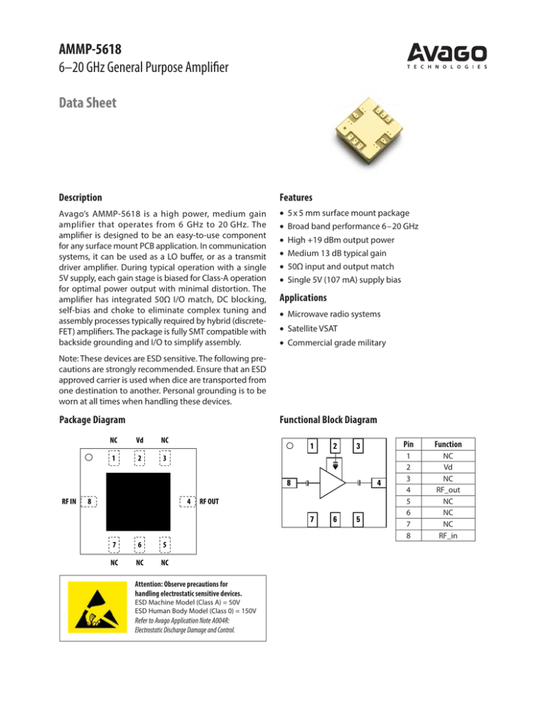
Package Diagram
NC
1
Functional Block Diagram
Vd
2
NC
1
2
3
3
4
8
RF IN
8
4
RF OUT
7
7
6
5
NC
NC
NC
Attention: Observe precautions for
handling electrostatic ­sensitive devices.
ESD Machine Model (Class A) = 50V
ESD Human Body Model (Class 0) = 150V
Refer to Avago Application Note A004R:
Electrostatic Discharge Damage and Control.
6
5
Pin
Function
1
2
3
4
5
6
7
8
NC
Vd
NC
RF_out
NC
NC
NC
RF_in
Electrical Specifications
1. Small/Large -signal data measured in a fully de-embedded test fixture form TA = 25°C, Vd=5V, Idq=107mA.
2. Pre-assembly into package performance verified 100% on-wafer per AMMC-5618 published specifications
3. This final package part performance is verified by a functional test correlated to actual performance at one or
more frequencies
4. Specifications are derived from measurements in a 50Ω test environment. Aspects of the amplifier performance
may be improved over a more narrow bandwidth by application of additional conjugate, linearity, or low noise
(Γopt) matching.
Table 1. RF Electrical Characteristics (TA= 25°C, Vd= 5.0V, Idq=107 mA, Zo=50 Ω)
Parameter
Typ.
Sigma
Unit
Frequency
Small-signal Gain, Gain
12
13
0.40
dB
5-6 GHz
Noise Figure into 50 Ω, NF
4.4
0.2
dB
Output Power at 1dB Gain Compression, P1dB
19
0.9
dBm
Third Order Intercept Point;
∆f=100MHz; Pin=-20dBm, OIP3
25
30
1.2
dBm
Input Return Loss, RLin
-12
0.7
dB
Output Return Loss, Rlout
-12
0.6
dB
Reverse Isolation, Isolation
-40
1.2
dB
5-6 GHz
Table 2. Recommended Operating Range
1. Ambient operational temperature TA = 25°C unless otherwise noted.
2. Channel-to-backside Thermal Resistance (Tchannel (Tc) = 34°C) as measured using infrared microscopy. Thermal
Resistance at backside temperature (Tb)= 25°C calculated from measured data.
Specifications
Description
Min.
Drain Supply Current, Id
Typical
Max.
Unit
Comments
107
140
mA
(Vd = 5 V, Under any RF power
drive and temperature
Table 3. Thermal Properties
Parameter
Test Conditions
Value
Thermal Resistance, qch-b
Backside Temperature, TA =25°C
qch-b = 34 °C/W
Absolute Minimum and Maximum Ratings
Table 4. Minimum and Maximum Ratings
Specifications
Description
Min.
Positive Drain Voltage, Vd
Max.
7
Unit
V
Drain Current, Id
150
mA
RF Input Power (Pin), RFin
20
dBm
Channel Temperature, Tch
Storage Temperature, Tstg
-65
Max. Assembly Temp, Tmax
+300
+150
°C
+150
°C
°C
Notes:
1. Operation in excess of any one of these conditions may result in permanent damage to this device.
2
Comments
CW
30 second maximum
Selected performance plots
15
0
12
-10
9
-20
S12 (dB)
S21 (dB)
These measurements are in 50Ω test environment at TA = 25°C, Vd = 5V, Id = 107 mA. Aspects of the amplifier performance may be improved over a narrower bandwidth by application of additional conjugate, linearity or low noise
(Γopt) matching.
6
-30
-40
3
0
4
6
8
10 12 14 16
FREQUENCY (GHz)
18
20
0
-5
-5
-10
-10
S22 (dB)
0
-15
-20
-25
-25
4
6
8
10 12 14 16
FREQUENCY (GHz)
18
20
-30
22
18
20
22
4
6
8
10 12 14 16
FREQUENCY (GHz)
18
20
22
30
7
25
OP-1dB (dBm)
NF (dB)
10 12 14 16
FREQUENCY (GHz)
35
8
6
5
4
20
15
10
OP1dB
OIP3
5
6
8
10
Figure 5. Noise Figure.
3
8
Figure 4. Output Return Loss.
Figure 3. Input Return Loss.
3
6
-15
-20
-30
4
Figure 2. Isolation.
Figure 1. Gain.
S11 (dB)
-50
22
12
14
16
FREQUENCY (GHz)
18
20
0
6
8
10
12
14
16
FREQUENCY (GHz)
Figure 6. Typical Power, OP-1dB and OIP3.
18
20
Over Temperature Performance Plots
These measurements are in 50Ω test environment at TA = 25°C, Vd = 5V, Id = 107 mA. Aspects of the amplifier performance may be improved over a narrower bandwidth by application of additional conjugate, linearity or low noise
(Γopt) matching.
20
0
15
-10
-20
S12 (dB)
S21 (dB)
10
5
-30
-40
25°C
−40°C
85°C
0
-5
4
6
8
10 12 14 16
FREQUENCY (GHz)
-50
18
20
-60
22
Figure 7. Gain Over Temperature.
4
6
8
10 12 14 16
FREQUENCY (GHz)
18
20
22
20
22
Figure 8. Isolation Over Temperature.
0
0
25°C
−40°C
85°C
25°C
−40°C
85°C
-5
-10
S22 (dB)
-5
S11 (dB)
25°C
−40°C
85°C
-10
-15
-20
-15
-20
-25
4
6
8
10 12 14 16
FREQUENCY (GHz)
18
20
-30
22
Figure 9. Input RL Over Temperature.
6
8
10 12 14 16
FREQUENCY (GHz)
108
25°C
−40°C
85°C
7
106
104
Idd (mA)
6
5
102
100
98
4
3
25°C
−40°C
85°C
96
6
8
10
12
14
16
FREQUENCY (GHz)
Figure 11. NF Over Temperature.
4
18
Figure 10. Output Return Loss Over Temperature.
8
NF (dB)
4
18
20
94
3
3.5
4
Vdd (V)
Figure 12. Bias Current Over Temperature.
4.5
5
Over Voltage plots
These measurements are in 50Ω test environment at TA = 25°C, Vd = 5V, Id = 107 mA. Aspects of the amplifier performance may be improved over a narrower bandwidth by application of additional conjugate, linearity or low noise
(Γopt) matching.
0
16
3V
4V
5V
-10
-20
S12 (dB)
S21 (dB)
12
8
-40
3V
4V
5V
4
0
-30
4
6
8
10 12 14 16
FREQUENCY (GHz)
-50
18
20
-60
22
0
3V
4V
5V
18
20
18
20
18
20
3V
4V
5V
-15
S22 (dB)
S11 (dB)
16
-10
-10
-20
-25
-30
4
6
8
10 12 14
FREQUENCY (GHz)
16
18
-35
20
Figure 15. Input RL Over Vdd.
4
6
8
10 12 14
FREQUENCY (GHz)
16
Figure 16. Output Return Loss Over Vdd.
35
20
30
16
25
12
OIP3 (dBm)
OP-1dB (dBm)
10 12 14
FREQUENCY (GHz)
-5
-15
8
6
8
10
12
14
16
FREQUENCY (GHz)
Figure 17. Output Power Over Vdd.
20
15
10
3V
4V
5V
4
5
8
0
-5
0
6
Figure 14. Isolation Over Vdd.
Figure 13. Gain Over Vdd.
-20
4
3V
4V
5V
5
18
20
0
6
8
10
12
14
16
FREQUENCY (GHz)
Figure 18. OIP3 Over Vdd.
Typical Scattering Parameters
Biasing and Operation
Please refer to <http://www.avagotech.com> for typical
scattering parameters data.
The AMMC-5618 is normally biased with a single positive
drain supply connected to both VD pins through bypass
capacitors as shown in Figure 19. The recommended
supply voltage is 5V. It is important to have 0.1 µF bypass
capacitor, and the capacitor should be placed as close to
the component as possible.
The AMMC-5618 does not require a negative gate voltage
to bias any of the two stages. No ground wires are
needed because all ground connections are made with
plated through-holes to the backside of the package.
Refer to the Absolute Maximum Ratings table for allowed
DC and thermal conditions.
Application Circuit
Vd
(Typ 5V)
0.1 F
1
RFin
2
3
RFout
4
8
7
6
Figure 21. Demonstration Board
(available upon request).
5
BASE
GND
Figure 19. Typical Application.
VD2
VD1
Feedback
Network
Feedback
Network
Matching
Matching
RF Input
RF Output
Matching
VG1
Figure 20. Simplified MMIC Schematic.
6
VG2
Package Dimension, PCB Layout and Tape and Reel information
Please refer to Avago Technologies Application Note 5520, AMxP-xxxx production Assembly Process (Land Pattern A).
Part Number Ordering Information
Part Number
Devices per Container
Container
AMMP-5618-BLK
10
antistatic bag
AMMP-5618-TR1
100
7” Reel
AMMP-5618-TR2
500
7” Reel
For product information and a complete list of distributors, please go to our web site:
www.avagotech.com
Avago, Avago Technologies, and the A logo are trademarks of Avago Technologies in the United States and other countries.
Data subject to change. Copyright © 2005-2013 Avago Technologies. All rights reserved. Obsoletes 5989-3545EN
AV02-0485EN - July 8, 2013


