User Guide 005
ZL8801-2PH-DEMO1Z Demonstration Board User Guide
The ZL8801 is a digital power conversion and management IC
that combines an efficient step-down DC/DC converter with
key power and thermal management functions in a single
package. The ZL8801 incorporates a fully digital,
compensation-free, ChargeMode™ control to achieve
single-cycle transient response.
The ZL8801-2PH-DEMO1Z demonstration board is a 6-layer
board demonstrating a 2-phase 80A synchronous buck
converter. Sequencing, margining, plus other features can be
evaluated using this demonstration board.
An USB-to-PMBus™ adapter board (ZLUSBEVAL3Z, included
with the demonstration kit) is used to connect the
demonstration board to a PC. Intersil’s PowerNavigator™
evaluation software can then be used to evaluate the full
PMBus functionality of the part using a PC running Microsoft
Windows XP, 7 or 8.
Specifications
• VIN = 12V
• VOUT = 1.2V/80A max
• fSW = 500kHz
• Efficiency: 91% at 40A
• Output ripple: ±1%
• Dynamic response: ±1% (50% to 100% to 50% load step,
di/dt = 10A/µs)
• Board temperature: +25°C
References
ZL8801 datasheet
ISL99140 datasheet
Key Features
Digital Power Design Center
• 2-phase 80A synchronous buck converter with
compensation-free ChargeMode control
AN1900, “USB to PMBus™ Adapter”
• Designed to be easy to use and modify. Optimized for small
circuit footprint and dynamic response
• Configurable through PMBus
• VIN range of 4.5V to 14V, VOUT adjustable from 0.54 to 2.0V
(Device can be adjusted to 5.5V with 6.3V output capacitors)
Ordering Information
PART NUMBER
DESCRIPTION
ZL8801-2PH-DEMO1Z ZL8801 Demonstration Kit (Evaluation Board,
USB Adapter, Cable)
• Enable switch and power-good indicator
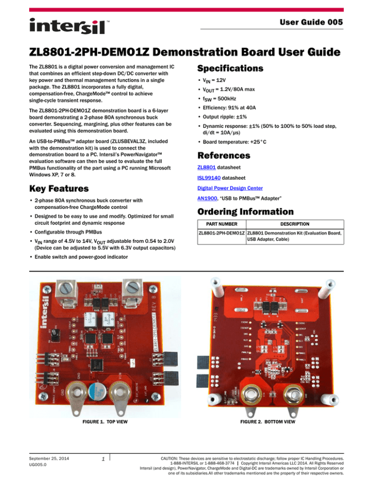
FIGURE 1. TOP VIEW
September 25, 2014
UG005.0
1
FIGURE 2. BOTTOM VIEW
CAUTION: These devices are sensitive to electrostatic discharge; follow proper IC Handling Procedures.
1-888-INTERSIL or 1-888-468-3774 | Copyright Intersil Americas LLC 2014. All Rights Reserved
Intersil (and design), PowerNavigator, ChargeMode and Digital-DC are trademarks owned by Intersil Corporation or
one of its subsidiaries.All other trademarks mentioned are the property of their respective owners.
User Guide 005
EN0
EN1
PWMH0
PG0
PG1
PWML0
VIN
ZL8801
CONTROL
AND
STATUS
VIN
VDRV
VDD
VDD
VIN
4.5V TO 14V
BST
PWM
ISL99140
EN
VSW
GND
VOUT
0.6V TO 5V
ISENA0
ISENB0
INTER-DEVICE
COMMUNICATION
DDC
VIN
PWMH1
VIN
VDD
VDRV
PWM
BST
ISL99140
SDA
SCL
SALRT
PMBus
PWML1
EN
VSW
GND
ISENA1
ISENB1
VSENP
VSENN
GND
FIGURE 3. ZL8801-2PH-DEMO1Z SIMPLIFIED SCHEMATIC
Functional Description
Operation
The ZL8801-2PH-DEMO1Z provides all circuitry required to
demonstrate the features of the ZL8801. The
ZL8801-2PH-DEMO1Z has a functionally-optimized ZL8801
circuit layout that allows efficient operation up to the maximum
output current.
PMBus Operation
A majority of the features of the ZL8801, such as
compensation-free ChargeMode control, soft-start delay and
ramp times, supply sequencing, voltage tracking and voltage
margining are available on this demonstration board. For voltage
tracking and sequencing demonstration, the board can be
connected to any other Intersil demonstration board that
supports the Digital-DC™ (DDC) bus.
Figure 3 shows a simplified schematic diagram of the
ZL8801-2PH-DEMO1Z board.
Install the evaluation software from the following Intersil
website:
http://www.intersil.com/powernavigator
The hardware enable function is controlled by a toggle switch on
the ZL8801-2PH-DEMO1Z board. The power-good (PG) LEDs
indicate the correct state of PG when external power is applied to
the ZL8801-2PH-DEMO1Z board. The right angle headers at
opposite ends of the board are for connecting a USB to PMBus
adapter board or for daisy chaining multiple demonstration
boards together to build multi-output configurations.
The evaluation software allows modification of all ZL8801
PMBus parameters. The ZL8801 device on the board has been
pre-configured as described in this document, but the user may
modify the operating parameters through the evaluation
software or by loading a predefined set-up from a configuration
file.
“ZL8801-2PH-DEMO1Z Schematic” on page 4 shows the detailed
demonstration circuit. Figures 5 through 11 show typical
performance data and Figures 16 through 23 show the PCB
board layout. The default configuration file is given on page 6,
and the Bill of Materials (BOM) is included for reference
beginning on page 5.
Submit Document Feedback
2
The ZL8801 utilizes the PMBus protocol. The PMBus functionality
can be controlled via USB from a PC running the PowerNavigator
evaluation software in Windows XP, 7 or 8 operating systems.
For board operation, connect the included USB-to-PMBus adapter
board to J8 of the ZL8801-2PH-DEMO1Z board labeled
“DONGLE”. Connect the desired load and an appropriate power
supply to the input and connect the included USB cable to the PC
running the PowerNavigator evaluation software. Place the
ENABLE switches in “DISABLE” and turn on the power.
The ENABLE switch can then be moved to “ENABLE” and the
ZL8801-2PH-DEMO1Z board can be tested. Alternately, the
PMBus ON_OFF_CONFIG and OPERATION commands may be
used from the PowerNavigator GUI.
UG005.0
September 25, 2014
User Guide 005
Quick Start Guide
USB (PMBus) Operation
1. Set ENABLE switch to “DISABLE”.
Stand Alone Operation
2. Apply load to VOUT and/or VOUT1.
1. Set ENABLE switch to “DISABLE”.
3. Connect power supply to VIN (supply turned off).
2. Apply load to VOUT0 and/or VOUT1.
3. Connect the USB to PMBus adapter board to J8 (labeled
“DONGLE”) of ZL8801-2PH-DEMO1Z.
4. Connect supplied USB cable from computer to USB to PMBus
adapter board.
5. Connect power supply to VIN (supply turned off).
6. Turn power supply on.
7. Set ENABLE switch to “ENABLE”.
8. Monitor ZL8801-2PH-DEMO1Z board operation using an
oscilloscope.
4. Turn power supply on.
5. Connect USB to PMBus adapter board to J8 of
ZL8801-2PH-DEMO1Z.
6. Connect supplied USB cable from computer to USB to PMBus
adapter board.
Install the PowerNavigator evaluation software from the
following Intersil website:
http://www.intersil.com/powernavigator
7. Set ENABLE switch to “ENABLE”.
8. Monitor and configure the ZL8801-2PH-DEMO1Z board using
PMBus commands in the evaluation software.
9. Test the ZL8801-2PH-DEMO1Z operation using an
oscilloscope and the evaluation software.
TO HOST COMPUTER
DEMO BOARD VIN
FIGURE 4. ZL8801 DEMONSTRATION KIT SET-UP
Submit Document Feedback
3
UG005.0
September 25, 2014
RL1632T4F-R002-FNH-01
EN1
SW_SPDT
4
1
C17
330u
16V
GND
3
6
PGND
C87
1.0uF
10K
C61
4.7uF
4.7uF
XTEMP1P
U9
2
17
18
EXT_VDRIVE
12
C58
13
R34
1
6
10
DS1
10K
PWMH1
PWML1
28.7k
2
VCC
SW1
VDRV
C74 C75
22uF 22uF
30
UVLO
VDRVEN
VMON
VSENP
VSENN
VSET
R25
31.6k
C62
C76
22uF
PWML1
42
8
9
10
11
12
13
14
4.7uF
R48
C64
DG
21
19
20
R47
OPEN
7
40
39
38
1
C65
4.7uF 4.7uF
392
ISEN1P
PGND
0.230uH
C88
1.0uF
PWMH1
L1
26
27
PG
SA
R38
R10
953
39
38
11
43
37
9
VTRKN
5
2
R36
665
VOUT
R33
1
C86 2
1.0uF
C77
1.0uF
ISEN1
VTRKP
LED
R18
C10 C11 C12 C4
C53 C78 C79 C80 C81 C82 C83 C84 470uF 470uF 470uF 470uF
2V
2V
2V
100uF 100uF 100uF 100uF 100uF 100uF 100uF 100uF 2V
C50
1.0uF
22
23
28
29
XTEMP1N
EXT_GND
PGND
NC_39
NC_38
NC_11
NC_43
NC_37
NC_9
ZL8801
1
5
37
41
16
17
18
19
20
21
22
23
24
25
26
27
28
XTEMP0N
2N3904
J6
PGND
PGND
PGND
PGND
PGND
PGND
PGND
PGND
PGND
PGND
PGND
PGND
PGND
VR6
ISENA0
ISENB0
ISENB1
ISENA1
XTEMP0P
C57
100pF
40
22uF
R12
953
MGN
VIN
VIN
VIN
VIN
VIN
VIN
VIN
VIN
PWM
EN
THDN
SMOD
PGND
Q6
ISL99140
2
Q2
ISEN0
L2
ISEN0P
GH1
VCC
BOARD TO BOARD INTERFACE
0.230uH
SW0
5
37
41
41
36
TP
AGND
AGND
AGND
16
0.1uF
EN
C51
100pF
2N3904
C49
7
43
15
29
30
31
32
33
34
35
PGND
SG
SGND
Q4
4
25
24
3
15
6
PWML0
VR5
SKT_3X2_RA
J10
GL
1
2
90.9k
PGND
3
CR1
DIODE_DUAL_C1_C2_CA
PGND
GH
BOOT
PHASE
SW
SW
SW
SW
SW
SW
SW
SW
SW
PGND
PGND
PGND
PGND
PGND
PGND
PGND
PGND
PGND
PGND
PGND
PGND
PGND
8
SCL
SDA
SALRT
DDC
SYNC
4
HDR_3X2_RA
42
Q3
16
17
18
19
20
21
22
23
24
25
26
27
28
1
2
3
4
5
6
SDA
SALRT
SCL
GND
Vi2c
MSTR_EN
PWMH0
PWML0
V25
1
2
3
4
5
6
PWMH0
IINP
EPAD
J8
SGND PGND
BOOT
PHASE
SW
SW
SW
SW
SW
SW
SW
SW
SW
ISL99140
PWM
EN
THDN
SMOD
GH0
GH
GL
6
4
7
43
15
29
30
31
32
33
34
35
C85
36
GL1
0.1uF
R37
1
J105
100
GND_1
User Guide 005
1
2
3
14
44
SGND
PGND
45
35
SKT_3X2_RA
IINN
VDD
34
32
HDR_3X2_RA
33
1
2
3
4
5
6
40
39
38
1
31
C60
J11
R43
R42
10K
10K
MSTR_SYNC
RSVD1
GND
DDC
RSVD2
RSVD3
36
1
2
3
4
5
6
PGND
R41
J9
R40
10K
C56
4.7uF
VIN
VIN
VIN
VIN
VIN
VIN
VIN
VIN
AGND
AGND
AGND
3
R49
42
8
9
10
11
12
13
14
PVCC
10K
PGND
C70 C71 C72
22uF 22uF 22uF
4
4
3
2
1
Disable
Open-Bus
Enable
PVCC
R7
2miliOhm 1W 4pin
C55
22uF
VIN
2
Submit Document Feedback
ZL8801-2PH-DEMO1Z Schematic
UG005.0
September 25, 2014
User Guide 005
Bill of Materials
QTY
REFERENCE DESIGNATOR
1
U9
2
DESCRIPTION
PCB FOOTPRINT
MANUFACTURER
PART NUMBER
ZL8801
QFN44_275X275
Intersil
ZL8801
Q3, Q6
ISL99140
QFN40_236X236
Intersil
ISL99140
1
CR1
BAT54A-T
SOT23
NXP Semiconductor
BAT54A, 215
4
C4, C10, C11, C12
470µF/2V
CAP_7343
Panasonic
EEF-SX0D471E4
1
C17
330µF
CAPAE_315X244
United Chemi-Con
APXA160ARA331MJC0G
2
C49, C85
0.1µF/16V/X7R
sm0402
TDK
C1005X7R1C104K050BC
5
C50, C77, C86, C87, C88
1.0µF/6.3V/X5R
sm0402
TDK
C1005X7S1A105K050BC
2
C51, C57
100pF/50V/COG-NPO
sm0402
TDK
C1005C0G1H101K050BA
8
C53, C78, C79, C80, C81, C82, C83, 100µF/6.3V/X5R
C84
sm1206
TDK
C3216X5R0J107M160AB
8
C55, C58, C70, C71, C72, C74, C75, 22µF/16V/X5R
C76
sm0805
TDK
C2012X5R1C226M085AC
4.7µF/16V/X5R
CAP_0603
TDK
C1608X5R1C475K080AC
6
C56, C60, C61, C62, C64, C65
2
L1, L2
0.230µH
IND_PA0511
Coil Craft
SLC1175-231ME_
2
Q2, Q4
2N3904
SOT23
On Semiconductor
MMBT3904LT1G
1
R7
2mΩ 1W 4pin
RL1632T4F
Cyntec
RL1632T4F-R002-F NH-01
2
R10, R12
953
SM0603
Panasonic
ERJ-3EKF9530V
1
R18
28.7k
SM0402
Panasonic
ERJ-2RKF2872X
1
R25
31.6k
SM0402
Panasonic
ERJ-2RKF3162X
1
R33
100
SM0402
Panasonic
ERJ-2RKF1000X
1
R36
665
SM0402
Panasonic
ERJ-2RKF6650X
1
R37
1
sm0603
Panasonic
ERJ-3RQF1R0V
1
R38
392
SM0402
Panasonic
ERJ-2RKF3920X
6
R40, R41, R42, R43, R49, R34
10k
SM0402
Panasonic
ERJ-2RKF1002X
0
R47
OPEN
SM0402
-
-
1
R48
90.9k
SM0402
Panasonic
ERJ-2RKF9092X
DEMONSTRATION BOARD SPECIFIC AUXILIARY PARTS BILL OF MATERIALS
1
DS1
LED
sm0805
Chicago Miniature
CMD17-21VGC/TR8
1
EN1
SW_SPDT (3 position)
SW_GT13MCBE
C&K Components
GT13MCBE
1
EXT_VDRIVE
T POINT S RED
TP_41C60P
Keystone Electronics
5000
1
EXT_GND
T POINT S BLACK
TP_41C60P
Keystone Electronics
5001
2
VIN, GND
Banana_J
BAN-JACK
Emerson
108-0740-00
2
GND_1, VOUT
LUG
B2C-PCB
Lugs Direct
B2C-PCB
2
J6, J105
2 POS
CONN2
Samtec
TSW-102-07-L-S
2
J8, J9
HDR_3X2_RA
CONN6
Samtec
TSW-103-08-T-D-RA
2
J10, J11
SKT_3X2_RA
CONN6
Samtec
SSQ-103-02-T-D-RA
Submit Document Feedback
5
UG005.0
September 25, 2014
User Guide 005
Configuration File
PCB Layout Guidelines
The following text is loaded into the ZL8801 device on the
ZL8801-2PH-DEMO1Z as default settings. Each PMBus
command is loaded via the PowerNavigator software. The #
symbol is used for a comment line.
For best performance with the ZL8801, please use the following
layout guidelines:
# Initialize device to factory settings
RESTORE_FACTORY
STORE_DEFAULT_ALL
STORE_USER_ALL
• DGND is the digital GND return path for the controller. It should
connect to the SGND shape using a single point, low
impedance connection.
• The VDD pin is the input supply pin for the ZL8801, and is also
used for VIN telemetry. The VR6, VR5 and V25 pins are outputs
of regulators used to bias internal circuitry. Ceramic
decoupling capacitors on these pins should be placed close to
their respective pin with a tight connection to SGND.
### Begin Default Store
RESTORE_DEFAULT_ALL
ON_OFF_CONFIG
0x17
VOUT_MAX
0x4000
#2V
VOUT_COMMAND
0x2000
#1V
VOUT_MARGIN_HIGH
0x219a
# 1.05 V
VOUT_MARGIN_LOW
0x1e66
# 0.95 V
FREQUENCY_SWITCH
0xfbe8
# 500 kHz
VOUT_OV_FAULT_LIMIT
0x235c
# 1.105 V
VOUT_UV_FAULT_LIMIT
0x1ca4
# 0.895 V
IOUT_OC_FAULT_LIMIT
0xe320
# 50 A
IOUT_UC_FAULT_LIMIT
0xe4e0
# -50 A
POWER_GOOD_ON
0x1ccd
IOUT0_CAL_GAIN
0xb11e
# 0.279 mV/A
IOUT1_CAL_GAIN
0xb11e
# 0.279 mV/A
USER_CONFIG
# 0.9 V
0x2686
IIN_CAL_GAIN
0xc300
DDC_CONFIG
0xa01
POWER_GOOD_DELAY
0xca00
INDUCTOR
# 3 mV/A
0xa7
DEADTIME_CONFIG
0x8888
ASCR_CONFIG
• The voltage sense lines should be routed differentially from the
regulation point back to the ZL8801. Be sure to avoid any
noisy areas when routing (such as the switch node) for best
performance.
• The current sense traces used for DCR sensing need to
connect to the inductor pads using a kelvin connection. This
minimizes stray PCB resistance in the current sense network,
maximizing current sense accuracy. The resistor in the RC
current sense network can be placed by the output inductor,
but the capacitor should be placed by the controller.
• The XTEMPxP and XTEMPxN signals should be routed as a
differential pair from the external NPN sensor back to the
controller, avoiding any noisy areas on the PCB. Up to a 100pF
capacitor can be placed across these pins for noise filtering.
• Ceramic input caps for the power stage need to be placed
close to the ISL99140 input pins, with a tight loop between the
ISL99140 VIN and PGND connections. The ceramic decoupling
capacitor for the ISL99140 VCC and PVCC pins should be
placed close to those pins.
• Please see the ZL8801 datasheet for guidance on component
selection, including input capacitors, output capacitors, and
the output inductor.
# 4 ms
0xb0eb
TEMPCO_CONFIG
SEQUENCE
• SGND is the analog reference for VDD, VR6, VR5 and V25 and
all pin-strap pins. It should connect to the system ground on
internal PCB layers. The ZL8801 paddle should then connect to
SGND with multiple vias for electrical and thermal relief.
# 0.229 uH
0x015a0190
0x0
DDC_GROUP
0x2fc00000
IOUT_AVG_OC_FAULT_LIMIT
0xe230
# 35 A
IOUT_AVG_UC_FAULT_LIMIT
0xe5d0
# -35 A
MFR_VMON_OV_FAULT_LIMIT
0xcb00
#6V
STORE_DEFAULT_ALL
### End Default Store
Submit Document Feedback
6
UG005.0
September 25, 2014
User Guide 005
The following data was acquired using a ZL8801-2PH-DEMO1Z demonstration board.
LOAD/MEASURED OUTPUT CURRENT (A)
Measured Data
90
80
70
60
LOAD CURRENT
50
40
MEASURED CURRENT
30
20
10
0
0
10
20
30
40
50
60
70
80
90
ACTUAL OUTPUT CURRENT (A)
FIGURE 5. OUTPUT CURRENT MEASUREMENT ACCURACY (SINGLE-PHASE)
95
95
90
93
91
80
1.0V
75
1.5V
1.2V
EFFICIENCY (%)
EFFICIENCY (%)
85
1.8V
0.8V
70
65
89
81
77
20
30
40
50
60
70
75
80
0
10
20
LOAD CURRENT (A)
95
95
90
90
85
85
75
1.5V
EFFICIENCY (%)
EFFICIENCY (%)
100
1.2V
40
50
60
FIGURE 7. EFFICIENCY, VIN = 5V, fSW = 300kHz
100
1.0V
30
LOAD CURRENT (A)
FIGURE 6. EFFICIENCY, VIN = 12V, fSW = 300kHz
80
1.8V
0.8V
79
10
1.5V
83
55
0
1.2V
85
60
50
1.0V
87
1.8V
0.8V
70
65
1.2V
1.5V
0.8V
1.8V
75
70
65
60
60
55
55
50
1.0V
80
50
0
10
20
30
40
50
60
70
LOAD CURRENT (A)
FIGURE 8. EFFICIENCY, VIN = 12V, fSW = 400kHz
Submit Document Feedback
7
80
0
10
20
30
40
50
60
LOAD CURRENT (A)
FIGURE 9. EFFICIENCY, VIN = 5V, fSW = 400kHz
UG005.0
September 25, 2014
User Guide 005
The following data was acquired using a ZL8801-2PH-DEMO1Z demonstration board. (Continued)
95
95
90
93
85
91
80
1.2V
1.0V
1.5V
EFFICIENCY (%)
EFFICIENCY (%)
Measured Data
1.8V
75
0.8V
70
65
89
87
79
77
10
20
30
40
50
60
70
80
LOAD CURRENT (A)
1.5V
0.8V
1.8V
81
55
0
1.2V
83
60
50
1.0V
85
75
0
10
20
30
40
50
60
LOAD CURRENT (A)
FIGURE 10. EFFICIENCY, VIN = 12V, fSW = 516kHz
FIGURE 11. EFFICIENCY, VIN = 5V, fSW = 516kHz
FIGURE 12. RAMP UP
FIGURE 13. RAMP DOWN
FIGURE 14. STEP RESPONSE, 20A TO 40A AT 5A/µs, ASCR = 1200
TOTAL DEVIATION WINDOW 25mV = 2.5%
FIGURE 15. STEP RESPONSE, 20A TO 40A AT 5A/µs, ASCR = 400
TOTAL DEVIATION WINDOW 50mV = 5%
Submit Document Feedback
8
UG005.0
September 25, 2014
User Guide 005
ZL8801-2PH-DEMO1Z Board Layout
FIGURE 16. PCB - TOP ASSEMBLY
FIGURE 17. PCB - TOP LAYER
FIGURE 18. PCB - INNER LAYER 1 (TOP VIEW)
FIGURE 19. PCB - INNER LAYER 2 (TOP VIEW)
Submit Document Feedback
9
UG005.0
September 25, 2014
User Guide 005
ZL8801-2PH-DEMO1Z Board Layout
(Continued)
FIGURE 20. PCB - INNER LAYER 3 (TOP VIEW)
FIGURE 21. PCB - INNER LAYER 4 (TOP VIEW)
FIGURE 22. PCB - BOTTOM LAYER (TOP VIEW)
FIGURE 23. PCB - BOTTOM ASSEMBLY (TOP VIEW)
Intersil Corporation reserves the right to make changes in circuit design, software and/or specifications at any time without notice. Accordingly, the reader is
cautioned to verify that the Application Note or Technical Brief is current before proceeding.
For information regarding Intersil Corporation and its products, see www.intersil.com
Submit Document Feedback
10
UG005.0
September 25, 2014
