IS31LT3352 MR16 DEMO Board Guide
Description
The IS31LT3352 is a continuous mode inductive
step-down converter, designed to efficiently drive a
single or multiple LEDs connected in series from a
voltage source higher than the total LED voltage. The
device can operate with an input voltage of 6V to 40V
and generate an output current of up to 750mA for a
total of 30W.
The IS31LT3352 includes an integrated output switch
and a high-side output current sensing circuit. An
external resistor is used to set the output current. It also
integrates a temperature compensation function in
order to maintain stable and reliable operation of the
LEDs’. The IS31LT3352 monitors the ambient
temperature near the LEDs with an external Negative
Temperature Coefficient (NTC) thermistor mounted
close to LEDs. The output current is automatically
reduced if the ambient temperature exceeds the
resistance threshold value set at RTH pin. The current
will return to the set value once the ambient
temperature goes below the threshold.
The IS31LT3352 can be connected in a serial chain all
using the same temperature compensation percentage.
In this chain, the device ADJO output pin will drive the
next IS31LT3352’s ADJI input pin with the temperature
compensation information. For this configuration a
single thermistor is required.
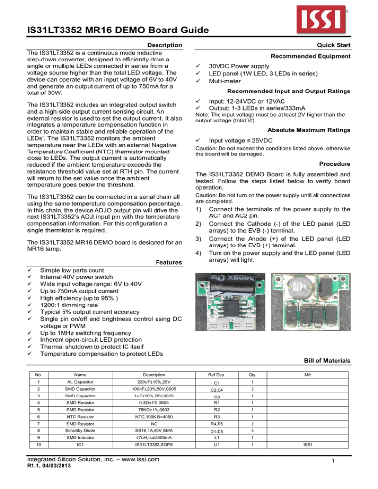
The IS31LT3352 MR16 DEMO board is designed for an
MR16 lamp.
Features
Quick Start
Recommended Equipment
30VDC Power supply
LED panel (1W LED, 3 LEDs in series)
Multi-meter
Recommended Input and Output Ratings
Input: 12-24VDC or 12VAC
Output: 1-3 LEDs in series/333mA
Note: The input voltage must be at least 2V higher than the
output voltage (total Vf).
Absolute Maximum Ratings
Input voltage ≤ 25VDC
Caution: Do not exceed the conditions listed above, otherwise
the board will be damaged.
Procedure
The IS31LT3352 DEMO Board is fully assembled and
tested. Follow the steps listed below to verify board
operation.
Caution: Do not turn on the power supply until all connections
are completed.
1)
2)
3)
4)
Connect the terminals of the power supply to the
AC1 and AC2 pin.
Connect the Cathode (-) of the LED panel (LED
arrays) to the EVB (-) terminal.
Connect the Anode (+) of the LED panel (LED
arrays) to the EVB (+) terminal.
Turn on the power supply and the LED panel (LED
arrays) will light.
Simple low parts count
Internal 40V power switch
Wide input voltage range: 6V to 40V
Up to 750mA output current
High efficiency (up to 95% )
1200:1 dimming rate
Typical 5% output current accuracy
Single pin on/off and brightness control using DC
voltage or PWM
Up to 1MHz switching frequency
Inherent open-circuit LED protection
Thermal shutdown to protect IC itself
Temperature compensation to protect LEDs
Bill of Materials
No.
Name
Description
Ref Des.
Qty.
1
AL Capacitor
220uF±10%,25V
C1
1
2
SMD Capacitor
100nF±20%,50V,0805
C2,C4
2
3
SMD Capacitor
1uF±10%,50V,0805
1
4
SMD Resistor
0.3Ω±1%,0805
C3
R1
5
SMD Resistor
75KΩ±1%,0603
R2
1
6
NTC Resistor
NTC,100K,B=4050
R3
1
7
SMD Resistor
NC
R4,R5
2
8
Schottky Diode
SS16,1A,60V,SMA
5
9
SMD Inductor
47uH,Isat≥600mA
D1-D5
L1
10
IC1
IS31LT3352,SOP8
U1
1
Integrated Silicon Solution, Inc. – www.issi.com
R1.1, 04/03/2013
Mfr
1
1
ISSI
1
IS31LT3352 MR16 DEMO Board Guide
R1
D2
D3
D5
1
AC/DC
C1
C2
6
ADJI
D1
D4
RTH
R2
LX
LT3352
SN3352
ADJO
RNTC
GND
4
7
R3
NTC
ISENSE
VIN
3
C3
2
L1
8
47uH
5
R2
temperature compensation point
75K
31ºC
33K
51ºC
20K
65ºC
C4
Figure 1 IS31LT3352 MR16 DEMO Board Schematic
Detailed Description
LED Current Control
The LED(s) output current is determined by the value of
the external current sense resistor (R1) connected
between VIN and ISENSE and is calculated by:
I OUT nom = 0.1/R1 [for R1>0.13Ω]
The table below lists examples of output current values
for various current set resistors (R1):
R1 (Ω)
Output current (mA)
0.13
0.15
0.27
0.3
769
667
370
333
The above values assume the ADJ pin is left floating at
a nominal voltage of VREF =1.2V.
Note that R1=0.13Ω is the minimum allowed value of
sense resistor in order to maintain the switch current
below the maximum allowable current.
Inductor selection
Recommended inductor values are in the range of
47μH to 220μH. The higher inductor values are
recommended for higher supply voltages and low
output currents in order to minimize variation in output
current over the supply voltage range. Higher
inductance values also minimize errors due to
switching delays, which cause increased ripple and
lower efficiency. The inductor should be mounted as
close to LX pin as possible.
Temperature compensation of output current
High luminance LEDs often need to be supplied with a
temperature compensated current in order to maintain
stable and reliable operation at all drive levels. The
LEDs are usually mounted remotely from the chip. If
output current compensation is required, it is possible
to use an external temperature sensing network normally using Negative Temperature Coefficient (NTC)
Integrated Silicon Solution, Inc. – www.issi.com
R1.1, 04/03/2013
thermistors and/or diodes, mounted very close to the
LED(s). The output of the sensing network can reduce
output current as the monitored LED temperature
increases.
As shown in Figure 2, temperature compensation is
decided by NTC thermistor R3 and resistor R2. When
the LED(s) temperature increases, thermistor
resistance of R3 starts to decrease. The temperature
compensation function is enabled once the NTC (R3)
resistance decreases to the point that the total
resistance (R3 + R4) equals the resistance of R2.
The equation for Iout current with temperature
compensation is:
In the case that 0.3< VADJI <1.2V:
I OUTdc = 0.083*VADJI(R3+R4)/R3*R2
In the case that VADJI >1.2V:
I OUTdc = 0.1*(R3+R4)/R2*R1
R3 and R4 decide the temperature compensation slope,
if R4 is 0Ω, the slope is decided by thermistor R3’s
parameter B-constant. A larger R4 resistance helps to
smooth out the slope.
Large R3 and R4 resistor values will require a larger R2
to match and vice versa. Too large resistance value for
R2 will make the Rth pin more sensitive to noise, too
small R4 resistance will increase IC current
consumption. An R2 resistance value of between 1K to
100K is recommended.
Figure 2 IS31LT3352 Temperature Compensation
An IS31LT3352 calculator is available from the ISSI to assist
with temperature compensation design.
2
IS31LT3352 MR16 DEMO Board Guide
PCB Layout
NOTE: Physical dimensions are (L x W x H): 18mm x 14mm x 10mm
Figure 2 PCB Layout-Top Layer
Figure 4 Component Placement Guide -Top Layer
Figure 3 PCB Layout-Bottom Layer
Figure 5 Component Placement Guide -Bottom Layer
Revision History
Date
Revision
Changes
2012.03.06
R1.0
Initial release
2012.04.12
R1.1
1. BOM: Add Cap tolerance value.
2. BOM: NTC B=3950 change to B=4050.
3. Change the temperature compensation point in the schematic table.
Copyright © 2013 Integrated Silicon Solution, Inc. All rights reserved. ISSI reserves the right to make changes to this specification and its
products at any time without notice. ISSI assumes no liability arising out of the application or use of any information, products or services
described herein. Customers are advised to obtain the latest version of this device specification before relying on any published information and
before placing orders for products.
Integrated Silicon Solution, Inc. – www.issi.com
R1.1, 04/03/2013
3
