MGA-412P8
GaAs Enhancement-mode pHEMT Power Amplifier
optimized for IEEE 802.11b/g applications
Data Sheet
Description
Features
Avago Technologies’s MGA-412P8 linear power amplifier is designed for applications in the (1.7-3) GHz
frequency range. The amplifier is optimized for IEEE
802.11b/g WLAN applications and has a best-in-class
efficiency (PAE) of 25.5% (54Mbps OFDM) achieved
through the use of Avago Technologies’ proprietary
GaAs Enhancement-mode pHEMT process.
• Advanced GaAs E-pHEMT
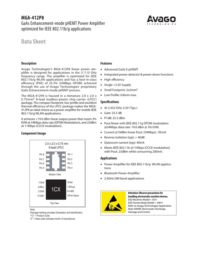
The MGA-412P8 is housed in a miniature 2.0 x 2.0 x
0.75mm 3 8-lead leadless-plastic-chip-carrier (LPCC)
package. The compact footprint, low profile and excellent
thermal efficiency of the LPCC package makes the MGA412P8 an ideal choice as a power amplifier for mobile IEEE
802.11b/g WLAN applications.
• Low Profile: 0.8mm max.
It achieves +19.0 dBm linear output power that meets 3%
EVM at 54Mbps data rate (OFDM Modulation), and 23dBm
at 11Mbps (CCCK modulation).
• P1dB: 25.3 dBm
Component Image
• Current @19dBm linear Pout: (54Mbps) : 95mA
• Integrated power detector & power down functions
• High efficiency
• Single +3.3V Supply
• Small Footprint: 2x2mm2
Specifications
• At 2.452 GHz; 3.3V (Typ.) :
• Gain: 25.5 dB
• Pout linear with IEEE 802.11g OFDM modulation
@54Mbps data rate: 19.0 dBm @ 3% EVM.
• Reverse Isolation (typ): > 40dB
2.0 x 2.0 x 0.75 mm
8-lead LPCC
Pin 8
Pin 1
Pin 7
Pin 2
Pin 6
Pin 3
Pin 5
Pin 4
• Quiescent current (typ): 40mA
• Meets IEEE 802.11b @11Mbps (CCCK modulation)
with Pout: 23dBm while consuming 200mA.
Applications
• Power Amplifier for IEEE 802.11b/g WLAN applications
• Bluetooth Power Amplifier
Bottom View
• 2.4GHz ISM band applications
8:Det
1:Gnd
2:RFin
2:Gnd
1CX
7:RFout
6:Vdd2
5:Pwr Down
4:Vdd1
Top View
Note:
Package marking provides Orientation and Identification
"1C" = Product Code
"X" = Date code indicates month of manufacture
Attention: Observe precautions for
handling electrostatic sensitive devices.
ESD Machine Model = 50 V
ESD Human Body Model = 200 V
Refer to Avago Technologies Application
Note A004R: Electrostatic Discharge,
Damage and Control.
Absolute Maximum Rating [1] Tc=25°C
Symbol
Parameter
Units
Absolute Max.
Vdd
Device Voltage, RF output to ground
V
5
Pin
CW RF Input Power (Vdd = 3.3V)
dBm
10
Pdiss
Total Power Dissipation [2]
W
0.8
Tj
Junction Temperature
oC
150
TSTG
Storage Temperature
oC
-65 to 150
Thermal Resistance [3]
(Vdd = 3.3V), θjc = 33.3 °C/W
Notes:
1. Operation of this device in excess of any of
these limits may cause permanent damage.
2. Board (package belly) temperature, Tb is 25 °C.
Derate 30mW/ °C for Tb>123.36 °C.
3. Thermal resistance measured using 150 °C
Liquid Crystal Measurement Technique.
Product Consistency Distribution Charts [4,5]
USL
30
35
40
45
50
55
Figure 1. Id@ 2.452GHz; Nominal = 40mA, USL: 55mA
LSL
24 24.2
24.6
25 25.2
25.6
26
Figure 2. P1dB @ 2.452GHz; Nominal = 25.3dBm, LSL: 24dBm
LSL
23
24
25
26
27
Figure 3. Gain@ 2.452GHz; Nominal = 25.5dB, LSL: 23 dB
28
Notes:
4. Distribution data sample size is 500 samples taken from 3 different
wafers and 3 different lots. Future wafers allocated to this product
may have nominal values anywhere between the upper and lower
limits.
5. Measurements are made on production test board, which represents
a trade-off between optimal Gain and P1dB. Circuit losses have been
de-embedded from actual measurements.
Electrical Specifications [6]
Tc = 25 °C, 2.452 GHz [typical, measured on demo board].DC bias for RF parameters Vdd =Vsd=3.3V
Unless otherwise specified, all data are taken with OFDM 64-QAM modulated signal per IEEE802.11g specifications
at 54Mbps data rate.
Symbol
Parameter
Units
Idq
Quiescent current
Isd
MIN
TYP
MAX
mA
40
55
Current drawn by Shutdown pin
mA
0.5
I_leak
Total current consumption at shutdown(Vsd=0V)
uA
5
G
Gain
dB
Psat
Saturated Power
dBm
P1dB
1 dB Compression Point
dBm
Gain Flatness (2.4 - 2.5GHz)
dB
1
Poutn
Max Pout per IEEE 802.11b mask (CCCK modulation)
dBm
23
Idn
Current @ 23dBm 802.11b BPSK
mA
200
Poutl
Linear Power @ 3% EVM, 54Mbps OFDM
dBm
19
Idl
Current @ 3% EVM
mA
95
S11
Input Return Loss
dB
-5.5
S22
Output Return Loss
dB
-11.5
S12
Isolation
dB
>40
OIP3
Large Signal, Output IP3 (2-tone at ± 10MHz from carrier freq)
dBm
38
23
25.5
27
24
25.3
Notes:
6. Measurements taken on demo board as shown on Figure 4. Excess circuit losses have been de-embedded from actual measurements. Standard
deviation and typical data based on at least 500 parts sample size from 2 wafer lots. Future wafers allocated to this product may have
nominal values any where within the upper and lower spec limits.
Demo board Diagram
DET
5.6nH
0ohm
5.6nH
6.8pF
1.2pF
6.8pF
INPUT
1.5pF
0.4mm
5.6nH
0.56mm
C
0ohm
1000pF
OUTPUT
2.2uF
22ohm
1000pF
0.1uF
OCT 2005
Rev 1.1
Figure 4. Demo board and Application Circuit Components
SD
18nH
Vdd
Schematic Diagram
Detector output
RF Input
P ort
P1
L
L5
L=5.6 nH
R=
L
L6
L=5.6 nH
R=
C
C1
C=6.8 pF
1
8
2
7
3
6
4
C
C3
C=1.2 pF
RF output
C
C
C2
C4
C=1.5 pF C=6.8 pF
P ort
P2
5
L
L3
L=5.6 nH
TLIN*
TL1
C
C7
C=2.2 uF
C
C5
C=1000 pF
Vshutdown = +3.3V ON
Vshutdown =0V OFF
C
C8
C=1000 pF
R
R1
R=22 Ohm
L
L4
L=18 nH
C
C6
C=0.1 uF
Vdd = +3.3V nom
Figure 5. Demo Board Schematic Diagram
* 0.56mm wide on 10mil thick Rogers RO4350 board
- Components L6, C2 and C3 should be located as close to the packaged device pins as possible.
- Components R1 and L4 are used to isolate the test board from Power Supply effects.
- Recommended PCB material is Roger, RO4350.
- Suggested component values may vary according to layout and PCB material.
MGA-412P8 Typical Performance I
Tc = +25 °C, Vdd = 3.3V Input Signal=CW unless stated otherwise.
Vdet vs Pout
Pout and Gain vs Pin
30
2.5
VDD=3V
2
VDD=3.3V
Pout
20
Gain
15
10
VDD=3.6V
1.5
Detector(V)
Pout(dBm) & Gain(dB)
25
1
5
0.5
0
-25
-20
-15
-10
-5
0
0
5
5
7
9
11
Input Power (dBm)
13
15
17
19
21
23
25
27
Output Power (dBm)
Figure 6. Output Power and Gain vs Input Power
Figure 7. Detector vs Output Power
MGA-412P8 Typical Performance II
EVM & Current vs Modulated Pout
160
EVM
140
Current
80
60
40
VDD=3.0V
VDD=3.3V
EVM(%)
120
100
EVM vs Modulated Pout
12
11
10
9
8
7
6
5
4
3
2
1
0
180
Current (mA)
12
11
10
9
8
7
6
5
4
3
2
1
0
20
0
5.0
6.0
7.0
8.0
9.0
10.0
11.0
12.0
13.0
14.0
15.0
16.0
17.0
18.0
19.0
20.0
21.0
22.0
23.0
24.0
EVM (%)
Tc = +25 °C, Vdd = 3.3V Input Signal=OFDM signal with 54Mbps, Modulation=64QAM unless stated otherwise.
VDD=3.6V
5
Modulated Output Power (dBm)
Figure 8. EVM & Current vs Output Power
160
23
25
PAE vs Modulated Output Power
40
VDD=3.6V
PAE%
100
80
60
30
20
40
10
20
0
0
5
7
9
11
13
15
17
19
21
Modulated Output Power(dBm)
Figure 10. Total Current vs Modulated Output Power
11
13
15
17
19
21
Modulated Output Power (dBm)
50
VDD=3.3V
120
IDD(mA)
60
VDD=3.0V
140
9
Figure 9. EVM vs Modulated Output Power
Total current vs Modulated Output Power
180
7
23
25
5 6 7 8 9 10 11 12 13 14 15 16 17 18 19 20 21 22 23 24
Modulated Output Power (dBm)
Figure 11. PAE vs Modulated Output Power
25 Deg C
-40 Deg C
85 Deg C
5
7
9
dB(S(2,1))
EVM(%)
EVM vs Modulated Output Power
12
11
10
9
8
7
6
5
4
3
2
1
0
11
13
15
17
19
21
Modulated Output Power (dBm)
23
25
27.0
26.5
26.0
25.5
25.0
24.5
24.0
23.5
23.0
22.5
22.0
2.40 2.42 2.44 2.46 2.48 2.50 2.52 2.54 2.56 2.58 2.60
freq, GHz
Figure 12. EVM vs Modulated Output Power at different Temperature
-4
dB(S(2,2))
dB(S(1,1))
-6
-8
-10
-12
2.40 2.42 2.44 2.46 2.48 2.50 2.52 2.54 2.56 2.58 2.60
freq, GHz
Figure 13. Typical Spectral Plot conforming compliance to IEEE 802.11b
11Mbps CCCK modulation mask at 23dBm output power
Figure 14. Typical Scattering Parameter Plots
2 x 2LPCC (JEDEC DFP-N) Package Dimensions
D1
D
pin1
P
pin1
1
8
2
7
e
E1
3
R
1CX
4
DIMENSIONS
E
6
5
b
L
Top View
Bottom View
A A1
A
A2
SYMBOL
A
A1
A2
b
D
D1
E
E1
e
P
L
MIN.
0.70
0
0.225
1.9
0.65
1.9
1.45
0.2
NOM.
0.75
0.02
0.203 REF
0.25
2.0
0.80
2.0
1.6
0.50 BSC
MAX.
0.80
0.05
0.25
0.3
0.275
2.1
0.95
2.1
1.75
0.4 REF
DIMENSIONS ARE IN MILLIMETERS
End View
End View
PCB Land Pattern and Stencil Design
2.72 (107.09)
2.80 (110.24)
0.70 (27.56)
0.63 (24.80)
0.25 (9.84)
0.22 (8.86)
0.25 (9.84)
PIN 1
0.50 (19.68)
0.50 (19.68)
0.20 (7.87)
Solder
mask
RF
transmission
line
0.32 (12.79)
PIN 1
1.54 (60.61)
1.60 (62.99)
0.28 (10.83)
+
0.60 (23.62)
0.25 (9.74)
0.63 (24.80)
0.72 (28.35)
0.80 (31.50)
0.15 (5.91)
0.55 (21.65)
Stencil Layout (top view)
PCB Land Pattern (top view)
Device Orientation
4 mm
REEL
8 mm
1CX
1CX
1CX
1CX
CARRIER
TAPE
USER
FEED
DIRECTION
COVER TAPE
Part Number Ordering Information
Part Number
No. of Devices
Container
MGA-412P8-TR1G
3000
7” Reel
MGA-412P8-TR2G
10000
13” Reel
MGA-412P8-BLKG
100
antistatic bag
For product information and a complete list of distributors, please go to our web site: www.avagotech.com
Avago, Avago Technologies, and the A logo are trademarks of Avago Technologies in the United States and other countries.
Data subject to change. Copyright © 2005-2008 Avago Technologies. All rights reserved. Obsoletes AV01-0236EN
AV02-0848EN - August 26, 2008


![dB = 10 log10 (P2/P1) dB = 20 log10 (V2/V1). dBm = 10 log (P [mW])](http://s2.studylib.net/store/data/018029789_1-223540e33bb385779125528ba7e80596-300x300.png)
