Selection Guide of SiC Schottky Diode in
CCM PFC Applications - August 2006
Selection Guide of SiC Schottky Diode in
CCM PFC Applications
Silicon Carbide Schottky diodes are ideal devices for CCM PFC boost diode applications because
of the superior reverse recovery characteristics – zero reverse recovery current. Selection of
a SiC Schottky boost diode is different from its counter part-- Silicon ultra fast soft recovery diode,
which is normally oversized due to the excessive reverse recovery energy loss. A Mathcad file
has been created in order to provide power supply designers a detailed explanation and calculation
on how to select appropriate SiC Schottkys for different power rated CCM PFC boost converters.
Introduction
Active power factor correction has been widely adopted in AC/DC Switch Mode Power Supply
(SMPS) designs due to the mandatory IEC-61000-4-3 requirements since January 2001. For SMPS
with output power rating higher than 300W, the active PFC boost converters are normally designed
to operate in Continuous Conduction Mode (CCM). The SiC Schottkys are ideal for this application.
Additionally, many lower power SMPS designs are adopting PFC in order to meet new efficiency standards.
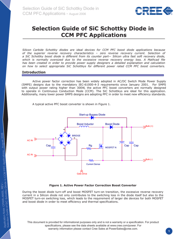
A typical active PFC boost converter is shown in Figure 1.
Start-up Bypass Diode
Boost Diode
+ 4
Bulk (+)
BRIDGE
3
1
AC IN
Cap
Rg
2 -
Vtions - August 2006
CPWR-AN05, RE
Application Note:
CCM PFC Applica
in
e
od
Di
y
ttk
ho
SiC Sc
Selection Guide of
Boost Inductor
MOSFET N
Cap
Cap
AC IN
Bulk (-)
Current Sense
Gate Drive
Figure 1. Active Power Factor Correction Boost Converter
During the boost diode turn-off and boost MOSFET turn-on transition, the excessive reverse recovery
current in a Silicon diode not only contributes to the switching loss in the diode itself but also to the
MOSFET turn-on switching loss, which leads to the requirement of larger die devices for both MOSFET
and boost diode in order to meet efficiency and thermal specifications.
This document is provided for informational purposes only and is not a warranty or a specification. For product
specifications, please see the data sheets available at www.cree.com/power. For
warranty information please contact Cree Sales at PowerSales@cree.com.
Selection Guide of SiC Schottky Diode in
CCM PFC Applications - August 2006
A Silicon Carbide Schottky diode is ideal for this application because of its virtual zero reverse
recovery current. The switching loss in the diode will be reduced drastically, as well as the turn-on switching
loss in the boost MOSFET. This will result in both boost MOSFET and diode die size reduction. Also, the snubber
circuit for the Silicon boost diode and MOSFET can usually be eliminated from the circuit. Use of SiC Schottky
diodes will provide a better overall system solution in terms of higher efficiency, less EMI noise, smaller heat
sink volume and PCB area. In addition, lower component count that not only reduces component cost, but will
also reduce material handling time, board assembly and in circuit testing time to save manufacturing cost.
SiC Schottky Diodes
Silicon Carbide is a wide bandgap, high breakdown field material allowing high voltage Schottky
diodes to be made. SiC Schottky diodes with 300, 600 and 1200-volt are commercially available at
CREE. The 600-volt diodes are available with 1, 2, 4, 6, 10 and 20-amp current ratings. The 1200-volt
diodes are available with 5, 10 and 20-amp current ratings. The main advantage of a high voltage SiC
Schottky diode lies in its superior dynamic performance. Schottky diodes are majority carrier devices
and thus do not store charge in their junctions. The reverse recovery charge in the SiC Schottky diode
is extremely low and is only the result of junction capacitance, not stored charge. Furthermore, unlike
the silicon PiN diode, the reverse recovery characteristics of SiC Schottkys are independent of di/dt,
forward current and junction temperature. The maximum junction temperature of 175°C in the SiC
Schottkys represents the actual operational temperature. The ultra-low junction charge in SiC Schottkys
results in reduced switching losses in a typical hard switched CCM PFC boost converter application.
The typical forward characteristics of a 10-amp SiC Schottky diode is as shown in Figure 2.
20
18
TJ
TJ
TJ
TJ
16
IF Forward Current (A)
14
=
=
=
=
25°C
75°C
125°C
175°C
12
10
8
6
4
2
0
0.0
0.5
1.0
1.5
2.0
2.5
3.0
3.5
VF Forward Voltage (V)
Figure 2. 10A/600V SiC Schottky Diode (CSD10060) Forward Characteristics
CPWR-AN05, REV Selection Guide of SiC Schottky Diode in
CCM PFC Applications - August 2006
This document is provided for informational purposes only and is not a warranty or a specification.
For product specifications, please see the data sheets available at www.cree.com/power.
For warranty information please contact Cree Sales at PowerSales@cree.com.
Selection Guide of SiC Schottky Diode in
CCM PFC Applications - August 2006
The SiC Schottky diode forward characteristics can be modeled as a temperature
dependant forward voltage source Vd and resistor Rd. Notice that the SiC Schottkys have
positive temperature coefficient that makes parallel operation of these devices an easy task.
Vd and Rd values at the given junction temperature can be calculated from the following equations.
Where a, b, Vd0, and Rd0 are extrapolated from the empirical forward characteristic measurement data.
The forward voltage drop of a SiC Schottky diode at any given forward bias current and given
junction temperature can be easily calculated from following equation, where Vd and Rd are calculated
from previous equations.
Power Loss Calculation of SiC Boost Diode in CCM PFC Applications
The calculation of power loss in the boost diode is important for two reasons. First, the current
handling capability of the diode is simply a function of the power loss and the operating junction temperature.
Thus by calculating the power loss, designers can be assured of choosing an adequately sized diode.
Second, the Mathcad program allows designers to choose a diode based upon their efficiency goals.
The power loss in the boost diode consists of conduction loss and switching loss. The conduction
loss is mainly caused by diode forward voltage drop at given forward bias current. The switching loss
is from the reverse recovery energy loss. In SiC Schottky diodes, the conduction loss is the main
power loss, and the switching loss is almost negligible since the reverse recovery current is near to
zero. However in silicon boost diode the reverse recovery energy loss is much higher compared to
conduction loss so that power supply designers have to choose much larger devices (both boost diode
and MOSFET) in order to meet efficiency and thermal requirements. To avoid common misconception
on replacing silicon diode with same current rating SiC devices, a step-by-step SiC Schottky boost
diode power loss Mathcad file has been created so as to give SMPS designers an insight on why and
how a much smaller current rating SiC Schottky diode can replace a much larger silicon boost diode.
The Mathcad file allows power supply designers to calculate the SiC Schottky boost diode power
loss with any given design specifications.
The calculation is based on the operation of CCM PFC boost converter. Assuming unity power
factor, the line current is in phase and shape with the input line voltage – a sinusoidal waveform, and the
PFC output voltage is DC.
The boost diode conduction loss is calculated from using the SiC schottky diode equivalent circuit
model of Vd in series with Rd. The switching loss is calculated from the energy loss caused by junction
capacitance charge at given operating voltage over one switching cycle and multiplying by the switching
frequency. Note that the loss caused by this capacitive charge is included in this loss model, however the
loss is usually seen in the boost MOSFET. The detailed calculation and derivation are given in the Mathcad
file: www.cree.com/products/power_docs.asp
CPWR-AN05, REV Selection Guide of SiC Schottky Diode in
CCM PFC Applications - August 2006
This document is provided for informational purposes only and is not a warranty or a specification.
For product specifications, please see the data sheets available at www.cree.com/power.
For warranty information please contact Cree Sales at PowerSales@cree.com.
Selection Guide of SiC Schottky Diode in
CCM PFC Applications - August 2006
The conduction loss of a SiC Schottky diode in a CCM PFC boost converter is as follows.
Where Io is the output current of the PFC converter, Vd and Rd are the equivalent resistance and forward
voltage drop at given junction temperature of the SiC Schottky diode, h is the expected efficiency of the
PFC converter, and Id_rms is the RMS current of the boost diode over one line cycle at given input voltage,
PFC output voltage and load current.
The switching loss of a SiC Schottky diode in a CCM PFC boost converter can be calculated from
following equation.
Where Qc is the total Schottky diode junction charge at specified voltage, Vo is the PFC output voltage,
and fs is the PFC converter switching frequency.
The over all diode loss in a CCM PFC boost converter is the summation of the conduction loss
and switching loss.
The junction temperature rise can be calculated based on the junction to case thermal resistance
given in the datasheets. The power supply designers can decide which Schottky diode should be used in
a specific PFC application so that the device is operating with certain thermal margin and also meeting
the efficiency specification.
Summary
Choosing a SiC Schottky boost diode is different from a Silicon diode due to the virtual zero
reverse recovery current of the SiC Schottkys. The calculation is simplified since the SiC Schottky reverse
recovery characteristics are independent from di/dt, forward bias current, and junction temperature. In
general, an oversized Silicon diode has to be chosen in PFC application in order to meet thermal and
efficiency requirements due to the excessive reverse recovery energy loss. In SiC Schottky case, the
diode current rating or die size can be reduced drastically in comparison to Silicon diode in a same power
rated PFC application. A Mathcad file has been created for the detailed equation derivation and power
loss calculation for power supply designers to choose appropriately rated SiC Schottky diodes for the
CCM PFC applications.
Copyright © 2006 Cree, Inc. All rights reserved. The information in this document is subject to change without notice. Cree, the Cree logo, and Zero
Recovery are registered trademarks of Cree, Inc.
This document is provided for informational purposes only and is not a warranty or a specification.
For product specifications, please see the data sheets available at www.cree.com/power.
For warranty information please contact Cree Sales at PowerSales@cree.com.
CPWR-AN05, REV Selection Guide of SiC Schottky Diode in CCM PFC Applications -August 2006
Cree, Inc.
4600 Silicon Drive
Durham, NC 27703
USA Tel: +1.919.313.5300
Fax: +1.919.313.5451
www.cree.com/power
