Enpirion® Power Datasheet
EN5336QI 3A PowerSoC
Voltage Mode Synchronous Buck
With Integrated Inductor
Output Voltage Programming
Description
Features
The EN5336QI is a Power System on Silicon DCDC converter. It is specifically designed to meet
the
precise voltage and fast transient
requirements of present and future highperformance, low-power processor, DSP, FPGA,
memory boards and system level applications in
a distributed power architecture. Advanced circuit
techniques, ultra high switching frequency, and
very advanced, high-density, integrated circuit
and proprietary inductor technology deliver highquality, ultra compact, non-isolated DC-DC
conversion. Operating this converter requires
only small value input and output ceramic
capacitors, a soft-start capacitor and a resistor
divider for voltage feedback to set the output
voltage to the desired value.
Altera’s Enpirion solution significantly helps in
system design and productivity by offering greatly
simplified
board
design,
layout
and
manufacturing requirements. In addition, a
reduction in the number of vendors required for
the complete power solution helps to enable an
overall system cost savings.
Altera’s Enpirion products are RoHS compliant
and
lead-free
manufacturing
environment
compatible.
PVIN
POK
VOUT
VOUT
AVIN
22F
XOV
SS
15 nF
Applications
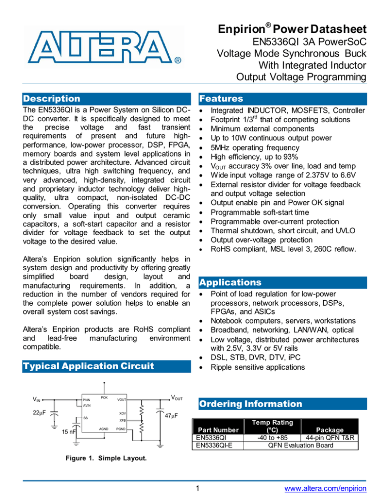
Typical Application Circuit
VIN
Integrated INDUCTOR, MOSFETS, Controller
Footprint 1/3rd that of competing solutions
Minimum external components
Up to 10W continuous output power
5MHz operating frequency
High efficiency, up to 93%
VOUT accuracy 3% over line, load and temp
Wide input voltage range of 2.375V to 6.6V
External resistor divider for voltage feedback
and output voltage selection
Output enable pin and Power OK signal
Programmable soft-start time
Programmable over-current protection
Thermal shutdown, short circuit, and UVLO
Output over-voltage protection
RoHS compliant, MSL level 3, 260C reflow.
Point of load regulation for low-power
processors, network processors, DSPs,
FPGAs, and ASICs
Notebook computers, servers, workstations
Broadband, networking, LAN/WAN, optical
Low voltage, distributed power architectures
with 2.5V, 3.3V or 5V rails
DSL, STB, DVR, DTV, iPC
Ripple sensitive applications
Ordering Information
47F
XFB
AGND
PGND
Part Number
EN5336QI
EN5336QI-E
Temp Rating
(°C)
Package
-40 to +85
44-pin QFN T&R
QFN Evaluation Board
Figure 1. Simple Layout.
1
www.altera.com/enpirion
EN5336QI
Pin Configuration
Below is a top view diagram of the EN5336QI package.
NOTE: NC pins are not to be electrically connected to each other or to any external signal, ground, or
voltage. However, they must be soldered to the PCB. Failure to follow this guideline may result in
part malfunction or damage.
Figure 2. Pin-out diagram, top view.
2
www.altera.com/enpirion
EN5336QI
Pin Descriptions
PIN
NAME
1-3
NC
4-6
NC(SW)
7
NC
8-14
VOUT
15
NC(SW)
16
NC
17-20
PGND
21-24
PVIN
25-26
NC
27
ROCP
28
AVIN
29
30-31
32
33
34
AGND
NC
XFB
XOV
NC
35
POK
36
NC
37
SS
38
39
EAIN
EAOUT
40
COMP
41
ENABLE
42-44
NC
FUNCTION
NO CONNECT – Do not electrically connect these pins to each other or to
PCB.
No Connect. These pins are internally connected to the switch node of the
internal MOSFETs. NC(SW) pins are not to be electrically connected to any
external signal, ground, or voltage.
No connect – Do not electrically connect these pins to each other or to PCB.
Regulated converter output. Connect these pins to the load and place output
capacitor from these pins the PGND pins 17-18
No Connect. These pins are internally connected to the switch node of the
internal MOSFETs. NC(SW) pins are not to be electrically connected to any
external signal, ground, or voltage.
No connect – Do not electrically connect these pins to each other or to PCB.
Output power ground. Connect these pins to the ground electrode of the
output filter capacitors. Refer to layout guideline section.
Input power supply. Connect to input power supply. Decouple with input
capacitor to PGND (pins 19-20).
No connect – Do not electrically connect these pins to each other or to PCB.
Optional Over Current Protection adjust pin. Place ROCP resistor between
this pin and AGND (pin 40) to increase the over current trip point by 50%.
Analog voltage input for the controller circuits. Connect this pin to the input
power supply.
Analog ground for the controller circuits.
No connect – Do not electrically connect these pins to each other or to PCB.
Voltage Feedback pin for external voltage divider network.
Optional Over-Voltage Programming Feedback pin.
No connect – Do not electrically connect these pins to each other or to PCB.
Power OK is an open drain transistor for power system state indication. POK
is a logic high when VOUT is with -10% to +20% of VOUT nominal.
No connect – Do not electrically connect these pins to each other or to PCB.
Soft-Start node. The soft-start capacitor is connected between this pin and
AGND. The value of this resistor determines the startup timing.
Optional Error Amplifier input. Allows for customization of the control loop.
Optional Error Amplifier output. Allows for customization of the control loop.
Optional Error Amplifier Buffer output. Allows for customization of the control
loop.
Input Enable. Applying a logic high, enables the output and initiates a softstart. Applying a logic low disables the output.
No connect – Do not electrically connect these pins to each other or to PCB.
3
www.altera.com/enpirion
EN5336QI
Block Diagram
POK
PVIN
power
Good
Logic
UVLO
Thermal Limit
ROCP
Current Limit
XOV
Over
Voltage
VOUT
Over Voltage
P-Drive
VOUT
(-)
N-Drive
PWM
Comp
(+)
PGND
Compensation
Network
Sawtooth
Generator
Voltage
Selector
(-)
Error
Amp
(+)
ENABLE
SS
XFB
Reference
Voltage
selector
Soft Start
Bandgap
Reference
COMP
EAIN
EAOUT
Figure 3. System block diagram.
Absolute Maximum Ratings
CAUTION: Absolute Maximum ratings are stress ratings only. Functional operation beyond
recommended operating conditions is not implied. Stress beyond Absolute maximum ratings may
cause permanent damage to the device. Exposure to absolute maximum rated conditions for
extended periods may affect device reliability.
Maximum Electrical Ratings
Min
Voltages on: V IN, VOUT
Voltages on XFB
Voltages on: ENABLE
Max
-0.3V
-0.3V
-0.3V
7.0V
2.5V
VIN + 0.3V
-40°C
-65°C
+85°C
+150°C
+260°C
Maximum Thermal Ratings
Ambient operating range
Storage Temperature Range
Reflow Peak Body Temperature MSL3 (10 Sec)
4
www.altera.com/enpirion
EN5336QI
Recommended Operating Conditions
PARAMETER
Input Voltage Range (for output voltages < 1.2V)
Input Voltage Range (for output voltages ≥ 1.2V)
EN5336QI Operating Ambient Temperature
Operating Junction Temperature
SYMBOL
VIN
VIN
TA
TJ
MIN
2.375
2.375
-40
-40
MAX
5.5
6.6
+85
+125
UNITS
V
V
°C
°C
Thermal Characteristics
SYMBOL
PARAMETER
TYP
UNITS
Thermal Shutdown
TSD
150
°C
Thermal Shutdown Hysteresis
TSDH
15
°C
Thermal Resistance: Junction to Case (0 LFM) (Note 1)
JC
3
°C/W
Thermal Resistance: Junction to Ambient (0 LFM)
JA
25
°C/W
Note 1: Based on a four-layer board and proper thermal design in line with JEDEC EIJ/JESD 51 Standards.
Electrical Characteristics
NOTE: VIN=5.5V over operating temperature range unless otherwise noted. Typical values are at T A =
25°C.
PARAMETER
Operating Input
Voltage (for output
voltages < 1.2V)
Operating Input
Voltage (for output
voltages ≥ 1.2V)
Feedback Pin Voltage
Drop out voltage
Shut-Down Supply
Current
Switching Frequency
SYMBOL
TEST CONDITIONS
MIN
TYP
MAX
UNITS
VIN
2.375
5.5
V
VIN
2.375
6.6
V
600
V
mV
VFB
VIN - VOUT
IS
0.75
Drop out voltage at full load
ENABLE=0V
FOSC
100
A
5
MHz
VOUT
Output Voltage
Regulation
VOUT
Over line, load and temperature
-3.0
3.0
%
Maximum Continuous Output Current
Over Current Trip
Piont
IOCP
4.5
A
Enable Operation
Disable Threshold
VDISABLE
Enable Threshold
VENABLE
Enable Pin Current
IENABLE
Max voltage to ensure the converter is
disabled
2.375V ≤ V IN ≤ 5.5V
5.5V < V IN
VIN = 5.5V
0.8
1.8
2.0
V
V
A
50
Voltage Select Operation
VSX Logic Low
Threshold
VSX-Low
Threshold voltage for Logic Low
VSX Logic High
Threshold
VSX-High
Threshold voltage for Logic High
(internally pulled high; can be left
floating to achieve logic high)
5
1.8
0.8
V
VIN
V
www.altera.com/enpirion
EN5336QI
PARAMETER
SYMBOL
VSX Pin Current
IVSX
TEST CONDITIONS
(VIN = 5.5V)
VSx = GND
VSx = V IN
VSx = Open
MIN
TYP
MAX
50
0
0
UNITS
A
Power OK Operation
POK low voltage
Max POK Voltage
VPOK
VPOK
IPOK = 4mA (sink current)
6
0.4
VIN
V
V
www.altera.com/enpirion
EN5336QI
Typical Performance Characteristics
VIN=5.0V
VIN=3.3V
95
90
VOUT = 2.5V
90
80
VOUT = 1.8V
75
VOUT = 1.5V
70
VOUT = 1.2V
65
Efficiency (%)
VOUT = 2.5V
85
Efficiency (%)
95
VOUT = 3.3V
85
VOUT = 1.8V
80
VOUT = 1.5V
75
VOUT = 1.2V
70
VOUT = 0.8V
65
60
60
55
55
50
50
0.1
0.3
0.5
0.7
0.9
1.1
1.3
1.5
1.7
1.9
2.1
2.3
2.5
2.7
0.1 0.3 0.5 0.7 0.9 1.1 1.3 1.5 1.7 1.9 2.1 2.3 2.5 2.7 2.9
2.9
Lo a d C urre nt ( A )
Lo a d C urre nt ( A )
Efficiency versus Load, VIN = 5.0V
Efficiency versus Load, VIN = 3.3V
Load transient, 0 – 3A, VIN/VOUT = 5.5V/1.2V
Load transient, 0 – 3A, VIN/VOUT = 5.5V/3.3V
Start-up waveform, VIN/VOUT = 5.5V/1.2V
Shut-down waveform, VIN/VOUT = 5.5V/1.2V
7
www.altera.com/enpirion
EN5336QI
Theory of Operation
set the resistor Ra1 for the desired output
voltage:
Synchronous Buck Converter
The
EN5336QI is
a synchronous, pin
programmable power supply with integrated
power MOSFET switches and integrated
inductor. The nominal input voltage range is 2.45.0V. The output can be set to any voltage
between 0.75V and VIN – 600mV. The feedback
control loop is a type III voltage-mode and the
part uses a low-noise PWM topology. Up to 3A of
output current can be drawn from this converter.
The 5MHz operating frequency enables the use
of small-size output capacitors.
The power supply has the following protection
features:
Over-current protection (to protect the IC
from excessive load current)
Thermal shutdown with hysteresis
Over-voltage protection
Under-voltage lockout circuit to disable the
converter output when the input voltage is
less than approximately 2.2V
Additional features include:
Soft-start circuit, limiting the in-rush
current when the converter is powered up
Power good circuit indicating whether the
output voltage is within 90% - 120% of the
programmed voltage
Ra1
(Vout 0.75V ) * Rb1
0.75V
If over-voltage protection is desired, use the
following equation to set the resistor Ra2 for the
desired OVP trip-point:
Ra 2
(OVPtrip 0.90V ) * Rb 2
0.90V
By design, if both resistor dividers are the same,
the OV trip-point will be 20% above the nominal
output voltage.
VIN
PVIN
POK
VOUT
VOUT
AVIN
Ra2
22F
Ra1
XOV
SS
CSS
47F
XFB
AGND
PGND
Rb2
Rb1
Figure 4. VOUT and OVP resistor divider networks.
NOTE: if no OVP divider is present, there will be
no over-voltage protection and POK will remain
“high” as long as VOUT remains above 90% of the
nominal VOUT setting.
Input Capacitor Selection
Output Voltage Programming
The EN5336QI output voltage is programmed
using a simple resistor divider network. Figure 4
shows the resistor divider configuration.
The EN5336QI output voltage and over voltage
thresholds are determined by the voltages
presented at the XFB and XOV pins respectively.
These voltages are set by way of resistor dividers
between VOUT and AGND with the midpoint going
to XFB and XOV.
The EN5336QI requires about 20uF of input
capacitance.
Low-cost,
low-ESR
ceramic
capacitors should be used as input capacitors for
this converter. The dielectric must be X5R or
X7R rated. In some applications, lower value
capacitors are needed in parallel with the larger,
capacitors in order to provide high frequency
decoupling. It is recommended to use 10V rated
MLCC capacitors. Table 2 lists some
recommended part numbers for input capacitors.
It is recommended that Rb1 and Rb2 resistor
values be ~2k. Use the following equation to
8
www.altera.com/enpirion
EN5336QI
Table 2. Recommended input capacitors.
Description
10uF, 10V, 10%
X7R, 1206
(2 capacitors needed)
22uF, 10V, 10%
X5R, 1210
(1 capacitor needed)
MFG
P/N
Murata
GRM31CR71A106KA01L
Taiyo Yuden
Murata
LMK316B7106KL-T
GRM32ER71A226KE20L
Taiyo Yuden
LMK325B7226KM-T
Output Capacitor Selection
The EN5336QI has been optimized for use with
approximately 50μF of output capacitance. Low
ESR ceramic capacitors are required with X5R or
X7R rated dielectric formulation.
Y5V or
equivalent dielectric formulations must not be
used as these lose capacitance with frequency,
temperature and bias voltage.
Output ripple voltage is determined by the
aggregate output capacitor impedance. Output
impedance, denoted as Z, is comprised of
effective series resistance, ESR, and effective
series inductance, ESL:
Z = ESR + ESL.
Placing output capacitors in parallel reduces the
impedance and will hence result in lower ripple
voltage.
1
Z Total
1
1
1
...
Z1 Z 2
Zn
Typical ripple versus capacitance is given below:
Output Capacitor
Configuration
1 x 47 uF
3 x 22 uF
Typical Output Ripple (mVp-p)
(as measured on EN5336QI
Evaluation Board)
30
15
Table 3. Recommended output capacitors.
Description
MFG
P/N
22uF, 6.3V, 10%
X5R, 1206
(3 capacitors needed)
47uF, 10V, 10%
X5R, 1210
47uF, 6.3V, 10%
X5R, 1210
(1 capacitor needed)
Murata
GRM31CR60J226KE19L
Taiyo Yuden
JMK316BJ226KL-T
Murata
GRM32ER61A476KE20L
AVX
12106D476KAT2
Enable Operation
The ENABLE pin provides a means to shut down
the device, or enable normal operation. A logic
high will enable the converter into normal
operation. When the ENABLE pin is asserted,
the device will undergo a normal soft start. A
logic low will disable the converter and cause it to
shut down. When Enable goes low, circuitry
internal to the device continue to operate to
ensure the output voltage is gradually returned to
zero and the circuits turn off subsequently. A
short low going pulse on Enable is ignored.
Soft-Start Operation
Soft start is a method to reduce in-rush current
when the device is enabled. The output voltage
is ramped up slowly upon start-up. The output
rise time is controlled by choice of a soft-start
capacitor, which is placed between the SS pin
(pin 37) and the AGND pin (pin 29).
Rise Time: TR = Css* 75K
During start-up of the converter, the reference
voltage to the error amplifier is gradually
increased from zero to its final level by an
internal current source of typically 10uA. Typical
soft-start rise time is 1mS to 3mS. The rise time
is measured from the time when AVIN > VUVLO
and the Enable signal crosses its logic high
threshold. Typical SS capacitor values are in the
range of 15nF to 50 nF.
Power-up Sequencing
The sequencing of AVIN, PVIN and ENABLE
should meet the following requirements:
1. ENABLE should not be asserted before PVIN.
2. PVIN should not be applied before AVIN.
Note that tying AVIN, PVIN and ENABLE
together and brought up at the same time does
meet these requirements.
POK Operation
The POK signal is an open drain signal from the
converter indicating the output voltage is within
the specified range. The POK signal will be a
logic high when the output voltage is above 90%
9
www.altera.com/enpirion
EN5336QI
of VOUT and below the user programmed OVP
trip-point. If the output voltage goes outside of
this range, the POK signal will be a logic low until
the output voltage has returned to within this
range. In the event of an over-voltage condition
the POK signal will go low and will remain in this
condition until the output voltage has dropped to
95% of the programmed output voltage before
returning to the high state.
NOTE: If no over voltage protection is used, POK
will remain “high” as long as VOUT remains above
90% of the nominal VOUT setting.
stops, the lower N-MOSFET is turned on and the
POK signal goes low. When the output voltage
drops below 95% of the programmed output
voltage, normal PWM operation resumes and
POK returns to its high state.
Thermal Overload Protection
Thermal shutdown will disable operation once
the Junction temperature exceeds approximately
150ºC. Once the junction temperature drops by
approx 25ºC, the converter will re-start with a
normal soft-start.
Over-Current Protection
Input Under-voltage Lock-out
The current limit function is achieved by sensing
the current flowing through the sense PMOSFET. When the sensed current exceeds the
current limit, both NFET and PFET switches are
turned off. If the over-current condition is
removed, the over-current protection circuit will
enable the PWM operation. This circuit is
designed to provide high noise immunity.
Circuitry is provided to ensure that when the
input voltage is below the specified voltage
range, the converter will not start-up. Circuits for
hysteresis, input de-glitch and output leading
edge blanking are included to ensure high noise
immunity and prevent false tripping.
The nominal over current trip point is set to 4.5A.
It is possible to increase the over-current set
point by about 50% by connecting a 7.5k
resistor between ROCP (pin 27) and GND. The
typical voltage at the ROCP pin is 0.75V.
In some cases, such as the start-up of FPGA
devices, it is desirable to blank the over-current
protection feature. In order to disable overcurrent protection, the ROCP pin should be tied
to any voltage between 2.5V and PVIN.
Over-Voltage Protection
Compensation
The EN5336QI is internally compensated
through the use of a type 3 compensation
network and is optimized for use with about 50uF
of output capacitance and will provide excellent
loop bandwidth and transient performance for
most applications. (See the section on Capacitor
Selection for details on recommended capacitor
types.) Voltage mode operation provides high
noise immunity at light load.
In some cases modifications to the compensation
may be required. For more information, contact
Power Applications support.
When the output voltage exceeds 120% of the
programmed output voltage, the PWM operation
10
www.altera.com/enpirion
EN5336QI
Layout Recommendation
Figure 4 shows critical components and layer 1
traces of a recommended minimum footprint
EN5336QI
layout.
Alternate
ENABLE
configurations and other small signal pins need
to be connected and routed according to specific
customer application. Please see the Gerber files
on the Altera website www.altera.com/enpirion
for exact dimensions and other layers. Please
refer to Figure 4 while reading the layout
recommendations in this section.
Recommendation 1: Input and output filter
capacitors should be placed on the same side of
the PCB, and as close to the EN5336QI package
as possible. They should be connected to the
device with very short and wide traces. Do not
use thermal reliefs or spokes when connecting
the capacitor pads to the respective nodes. The
+V and GND traces between the capacitors and
the EN5336QI should be as close to each other
as possible so that the gap between the two
nodes is minimized, even under the capacitors.
Recommendation 2: Two PGND pins are
dedicated to the input circuit, and two to the
output circuit. The slit in Figure 4 separating the
input and output GND circuits helps minimize
noise coupling between the converter input and
output switching loops.
Recommendation 3: The system ground plane
should be the first layer immediately below the
surface layer. This ground plane should be
continuous
and un-interrupted below the
converter and the input/output capacitors. Please
see the Gerber files on the Altera website
www.altera.com/enpirion.
Recommendation 4: The large thermal pad
underneath the component must be connected to
the system ground plane through as many vias
as possible.
Figure 4: Top PCB Layer Critical Components
and Copper for Minimum Footprint
The drill diameter of the vias should be 0.33mm,
and the vias must have at least 1 oz. copper
plating on the inside wall, making the finished
hole size around 0.20-0.26mm. Do not use
thermal reliefs or spokes to connect the vias to
the ground plane. This connection provides the
path for heat dissipation from the converter.
Please see Figures: 7, 8, and 9.
Recommendation 5: Multiple small vias (the
same size as the thermal vias discussed in
recommendation 4 should be used to connect
ground terminal of the input capacitor and output
capacitors to the system ground plane. It is
preferred to put these vias under the capacitors
along the edge of the GND copper closest to the
+V copper. Please see Figure 4. These vias
connect the input/output filter capacitors to the
GND plane, and help reduce parasitic
inductances in the input and output current loops.
If the vias cannot be placed under C IN and COUT ,
then put them just outside the capacitors along
the GND slit separating the two components. Do
not use thermal reliefs or spokes to connect
these vias to the ground plane.
Recommendation 6: AVIN is the power supply
for the internal small-signal control circuits. It
should be connected to the input voltage at a
11
www.altera.com/enpirion
EN5336QI
quiet point. In Figure 4 this connection is made at
the input capacitor close to the VIN connection.
Recommendation 7: The layer 1 metal under
the device must not be more than shown in
Figure 4. See the section regarding exposed
metal on bottom of package. As with any switchmode DC/DC converter, try not to run sensitive
signal or control lines underneath the converter
package on other layers.
Recommendation 8: The external feedback
resistor sense point (top feedback resistor)
should be just after the last output filter capacitor.
Keep the sense trace as short as possible in
order to avoid noise coupling into the control
loop. Place the feedback resistor components
near the XFB pin. The ground for the external
feedback resistor should be connected to a quiet
ground such as AGND.
12
www.altera.com/enpirion
EN5336QI
Design Considerations for Lead-Frame Based Modules
Exposed Metal on Bottom of Package
Lead frame offers many advantages in thermal performance, in reduced electrical lead resistance,
and in overall foot print. However, they do require some special considerations.
In the assembly process lead frame construction requires that, for mechanical support, some of the
lead-frame cantilevers be exposed at the point where wire-bond or internal passives are attached.
This results in several small pads being exposed on the bottom of the package.
Only the large thermal pad and the perimeter pads are to be mechanically or electrically connected to
the PC board. The PCB top layer under the EN5336QI should be clear of any metal except for the
large thermal pad. The “grayed-out” area in Figure 5 represents the area that should be clear of any
metal (traces, vias, or planes), on the top layer of the PCB. Figure 6 shows the rec ommended PCB
footprint for this device.
Figure 5. Lead-Frame exposed metal. Grey area highlights exposed metal that is not to be mechanically or
electrically connected to the PCB.
13
www.altera.com/enpirion
EN5336QI
Figure 6: EN5336QI PCB Footprint (Top View)
The solder stencil aperture for the thermal pad is shown in blue and is based on Enpirion power product manufacturing
specifications.
14
www.altera.com/enpirion
EN5336QI
Package Dimensions
Figure 7. Package dimensions.
Contact Information
Altera Corporation
101 Innovation Drive
San Jose, CA 95134
Phone: 408-544-7000
www.altera.com
© 2013 Altera Corporation—Confidential. All rights reserved. ALTERA, ARRIA, CYCLONE, ENPIRION, HARDCOPY, MAX, MEGACORE, NIOS,
QUARTUS and STRATIX words and logos are trademarks of Altera Corporation and registered in the U.S. Patent and Trademark Office a nd in other
countries. All other words and logos identified as trademarks or service marks are the property of their respective hol ders as described at
www.altera.com/common/legal.html. Altera warrants performance of its semiconductor products to current specifications in accordance with Altera's
standard warranty, but reserves the right to make changes to any products and services at any time without notice. Altera assumes no responsibility or
liability arising out of the application or use of any information, product, or service described herein except as expressly agreed to in writing by Altera.
Altera customers are advised to obtain the latest version of device specifications before relying on any published information and before placing orders
for products or services.
15
www.altera.com/enpirion


