LR12
LR12
Initial Release
High Input Voltage
Adjustable 3-Terminal Linear Regulator
Features
General Description
❏
❏
❏
❏
❏
❏
❏
❏
The Supertex LR12 is a high voltage, low output current,
adjustable linear regulator. It has a wide operating input voltage
range of 13.2V to 100V. The output voltage can be adjusted from
1.20V to 88V provided that the input voltage is at least 12V
greater than the output voltage. The output voltage can be
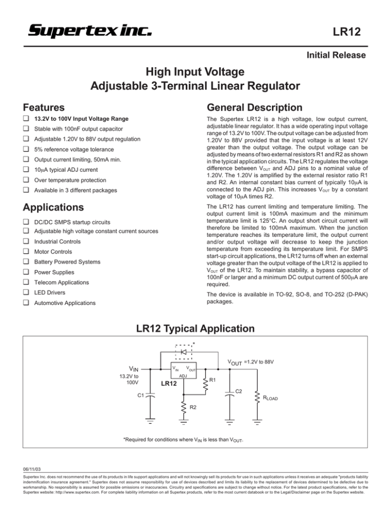
adjusted by means of two external resistors R1 and R2 as shown
in the typical application circuits. The LR12 regulates the voltage
difference between VOUT and ADJ pins to a nominal value of
1.20V. The 1.20V is amplified by the external resistor ratio R1
and R2. An internal constant bias current of typically 10µA is
connected to the ADJ pin. This increases VOUT by a constant
voltage of 10µA times R2.
13.2V to 100V Input Voltage Range
Stable with 100nF output capacitor
Adjustable 1.20V to 88V output regulation
5% reference voltage tolerance
Output current limiting, 50mA min.
10µA typical ADJ current
Over temperature protection
Available in 3 different packages
Applications
❏
❏
❏
❏
❏
❏
❏
❏
❏
The LR12 has current limiting and temperature limiting. The
output current limit is 100mA maximum and the minimum
temperature limit is 125°C. An output short circuit current will
therefore be limited to 100mA maximum. When the junction
temperature reaches its temperature limit, the output current
and/or output voltage will decrease to keep the junction
temperature from exceeding its temperature limit. For SMPS
start-up circuit applications, the LR12 turns off when an external
voltage greater than the output voltage of the LR12 is applied to
VOUT of the LR12. To maintain stability, a bypass capacitor of
100nF or larger and a minimum DC output current of 500µA are
required.
DC/DC SMPS startup circuits
Adjustable high voltage constant current sources
Industrial Controls
Motor Controls
Battery Powered Systems
Power Supplies
Telecom Applications
LED Drivers
The device is available in TO-92, SO-8, and TO-252 (D-PAK)
packages.
Automotive Applications
LR12 Typical Application
*
VIN
13.2V to
100V
VIN
VOUT =1.2V to 88V
VOUT
ADJ
R1
LR12
C2
C1
RLOAD
R2
*Required for conditions where VIN is less than VOUT.
06/11/03
Supertex Inc. does not recommend the use of its products in life support applications and will not knowingly sell its products for use in such applications unless it receives an adequate "products liability
indemnification insurance agreement." Supertex does not assume responsibility for use of devices described and limits its liability to the replacement of devices determined to be defective due to
workmanship. No responsibility is assumed for possible omissions or inaccuracies. Circuitry and specifications are subject to change without notice. For the latest product specifications, refer to the
Supertex website: http://www.supertex.com. For complete liability information on all Supertex products,
1 refer to the most current databook or to the Legal/Disclaimer page on the Supertex website.
LR12
Ordering Information
Package Options
SO-8
TO-252
TO-92
LR12LG
LR12K4
LR12N3
Pin Configurations
Absolute Maximum Ratings
VIN-ADJ
-0.5V to +120V
VOUT-ADJ
VOUT
ADJ
NC
NC
VIN
-10V to +10V
VIN – VOUT
-0.5V to +120V
Operating Ambient Temperature Range
-40°C to +85°C
Operating Junction Temperature Range
-40°C to +125°C
Storage Temperature Range
-65°C to +150°C
1
8
2
7
3
6
4
5
VOUT
VOUT
VOUT
VOUT
VIN
ADJ
TO-252
(D-PAK)
SO-8
ADJ
VOUT
VIN
TO-92
Electrical Characteristics
Test conditions unless otherwise specified: -40°C < TA < 85°C.
Symbol
Parameter
Min
VIN - VOUT
Input to Output Voltage Difference
12
VOUT
Overall Output Voltage Regulation
1.14
∆VOUT
Typ
Max
Units
98.8
V
1.20
1.26
V
Line Regulation
0.003
0.01
%/V
15V<VIN<100V, VOUT=5V, IOUT=0.5mA
∆VOUT
Load Regulation
1.4
3.0
%
VIN=15V, VOUT=5V, 0.5mA<IOUT<50mA
∆VOUT
Temperature Regulation
+1
%
VIN=15V, VOUT=5V, IOUT=10mA,
-1
Test Conditions
13.2V<VIN<100V, R1=2.4KΩ, R2=0
-40°C<TA<85°C
IOUT
Output Current Limit
IOUT
Output Current Limit
IOUT
Minimum Output Current
IADJ
Adjust Output Current
C2
Minimum Output Load Capacitance
DVOUT/DVIN Ripple Rejection Ratio
TLIMIT
Junction Temperature Limit
50
100
mA
TJ < 85°C, VIN - VOUT = 12V
0.5
mA
TJ > 125°C, VIN - VOUT = 100V
mA
Includes R1 and load current
0.5
5
10
100
50
15
µA
nF
60
125
dB
°C
2
120Hz, VOUT = 5V
LR12
Thermal Characteristics
Power Dissipation
@ TA=25°C
θJC
θJA
°C/W
°C/W
TO-92
0.6W
125
170
SO-8
1.8W
—
55†
TO-252
2.0W
6.25
50†
Package
†
Mounted on FR4 board, 25mm x 25mm x 1.57mm.
Significant PD increase possible on ceramic substrate.
Functional Block Diagram
VIN
LR12
Pass
Element
Overtemp &
Overcurrent
VOUT
6.5V
1KΩ
1.2V
3
10µA
ADJ
LR12
Typical Application Circuits
*
V
VIN=17V to 100V
VOUT=5.0V
VOUT
IN
ADJ
R1
6.04KΩ
±1%
LR12
C1
C2
100nF
RLOAD ≤16.5KΩ
R2
18.2KΩ
±1%
VOUT = 1.20V 1+ R2 + IADJ R2
R1
Figure 1: High Input Voltage, 5.0V Output Linear Regulator
* Required for conditions where VIN is less than VOUT.
VIN=15V to 100V
+
VAuxiliary
Vout1
-
LR12
VIN
+
VOUT
ADJ
Vout2
-
Vcc
FB
PWM IC
Figure 2: SMPS Start-Up Circuit
IOUT =
LR12
+
VIN
1.20V
R
VOUT
R
ADJ
VIN = 15V
to 100V
100nF
-
Figure 3: High Voltage Adjustable Constant Current Source
4
LR12
Typical Performance Curves
Temperature Variation
1.30
VIN
1.25
LR12
ADJ
2.4KΩ
13.2V
100nF
VOUT (V)
VOUT=1.2V
1.20
1.15
1.10
1.05
1.00
-50
-25
0
25
50
75
100
125
T(junction) (°C)
Load Regulation
5.30
5.25
VIN
VOUT=5.0V
IOUT
5.20
LR12
5.15
6.04KΩ
±1%
100nF
25V
VOUT (V)
ADJ
RLOAD
18.2KΩ
±1%
5.10
5.05
5.00
4.95
4.90
4.85
4.80
0
5
10
15
20
25
30
IOUT (mA)
5
35
40
45
50
LR12
Typical Performance Curves
VOUT vs. VIN
6
V
V
IN
OUT
=5.0V
5
ADJ
VOUT (V)
LR12
6.04KΩ
±1%
100nF
0V to 50V
1KΩ
18.2KΩ
±1%
4
3
2
1
0
0
20
40
60
80
100
VIN (V)
Ripple Rejection
-65
IOUT
Ripple Rejection Ratio (dB)
VOUT =5.0V
VIN
LR12
20VP-P
@ 120Hz
ADJ
6.04KΩ
±1%
100nF
RLOAD
65V
18.2KΩ
±1%
-64
-63
-62
-61
-60
0
10
20
30
40
IOUT (mA)
Current Limit
100
Ic (mA)
90
80
70
60
50
-40
-20
0
20
40
Temperature (°C)
6
60
80
100
50
LR12
Typical Performance Curves
Load Transient Response
V
SW
VOUT=5.0V
IN
Closed
LR12
ADJ
6.04KΩ
±1%
SW
100nF
25V
Open
10KΩ
18.2KΩ
±1%
509Ω
VOUT
200mV/div
Load Transient Response, Load=509Ω
Line Transient Response
100V
VOUT
VIN
VIN
LR12
0V
ADJ
6.04KΩ
±1%
100nF
10KΩ
18.2KΩ
±1%
VIN
50V/div
VOUT
5V/div
Line Turn On/Off Response
VIN
50V/div
VIN
50V/div
VOUT
5V/div
VOUT
5V/div
Line Power Up Transient
Line Power Down Transient
06/16/03rev.5
©2003 Supertex Inc. All rights reserved. Unauthorized use or reproduction prohibited.
7
1235 Bordeaux Drive, Sunnyvale, CA 94089
TEL: (408) 222-8888 • FAX: (408) 222-4895
www.supertex.com


