EC4304 1A, Hysteretic, High Brightness LED Driver with - E-CMOS
advertisement

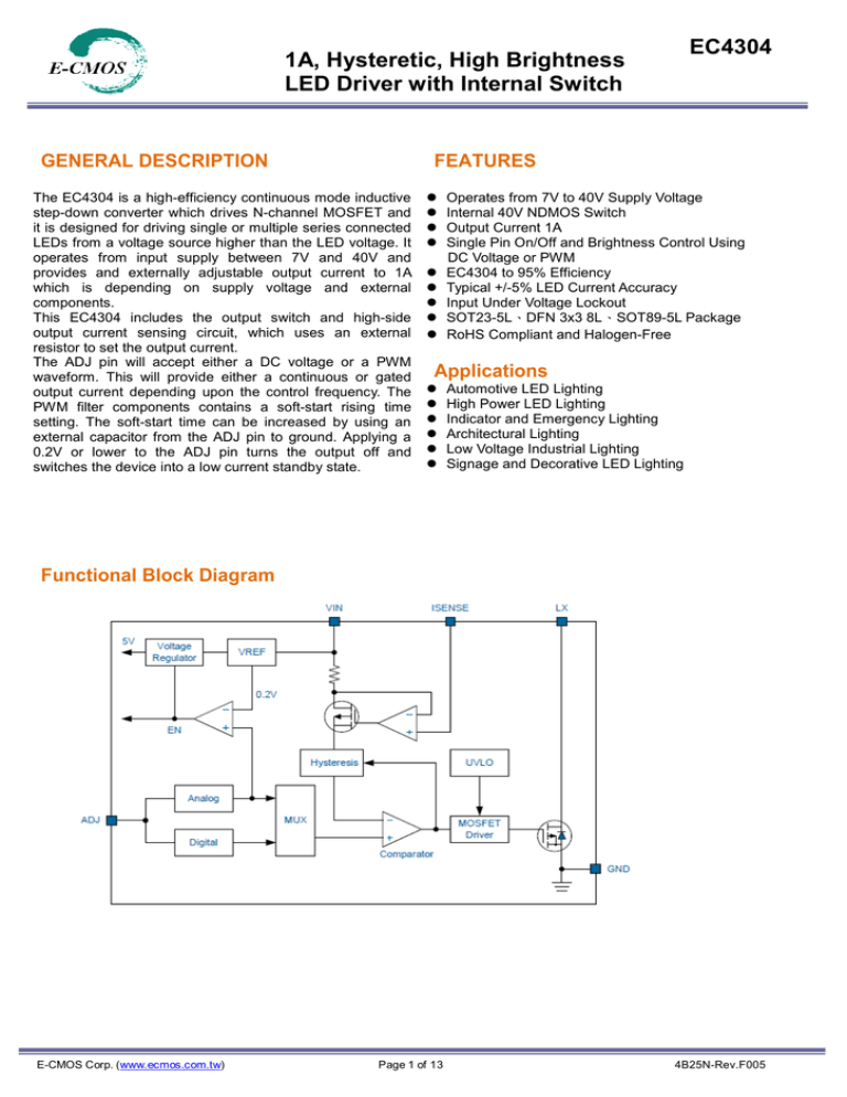
EC4304 1A, Hysteretic, High Brightness LED Driver with Internal Switch GENERAL DESCRIPTION FEATURES The EC4304 is a high-efficiency continuous mode inductive step-down converter which drives N-channel MOSFET and it is designed for driving single or multiple series connected LEDs from a voltage source higher than the LED voltage. It operates from input supply between 7V and 40V and provides and externally adjustable output current to 1A which is depending on supply voltage and external components. This EC4304 includes the output switch and high-side output current sensing circuit, which uses an external resistor to set the output current. The ADJ pin will accept either a DC voltage or a PWM waveform. This will provide either a continuous or gated output current depending upon the control frequency. The PWM filter components contains a soft-start rising time setting. The soft-start time can be increased by using an external capacitor from the ADJ pin to ground. Applying a 0.2V or lower to the ADJ pin turns the output off and switches the device into a low current standby state. Operates from 7V to 40V Supply Voltage Internal 40V NDMOS Switch Output Current 1A Single Pin On/Off and Brightness Control Using DC Voltage or PWM EC4304 to 95% Efficiency Typical +/-5% LED Current Accuracy Input Under Voltage Lockout SOT23-5L、DFN 3x3 8L、SOT89-5L Package RoHS Compliant and Halogen-Free Applications Automotive LED Lighting High Power LED Lighting Indicator and Emergency Lighting Architectural Lighting Low Voltage Industrial Lighting Signage and Decorative LED Lighting Functional Block Diagram E-CMOS Corp. (www.ecmos.com.tw) Page 1 of 13 4B25N-Rev.F005 1A, Hysteretic, High Brightness LED Driver with Internal Switch EC4304 Pin Configuration Pin Name LX GND ADJ ISENSE VIN Pin Function Drain of NDMOS Switch. Ground for the IC. All voltages levels are measured with respect to this pin. Multi-Function ON/OFF and Brightness Control Pin: -Analog signal input for analog control of PWM dimming. -PWM signal input for digital PWM dimming. Current Sense Pin: Sense LED String Current. Power supply input pin. Connect a nominal (7V~40V) power supply to this pin. The power- on-reset (POR) function monitors the input voltage by this pin. It is recommended that a decoupling capacitor (4.7µF or Higher X7R Ceramic capacitor) be connected to the GND for noise decoupling. Typical Application E-CMOS Corp. (www.ecmos.com.tw) Page 2 of 13 4B25N-Rev.F005 EC4304 1A, Hysteretic, High Brightness LED Driver with Internal Switch Ordering/ Marking Information Part Number Package Marking EC4304ANT2R SOT23-5 4304A LLLLLL EC4304ANFNR DFN3x3-8 EC4304ANB9R SOT89-5L E-CMOS Corp. (www.ecmos.com.tw) Page 3 of 13 4304A YWLLL Marking Information LLLLLL is Lot No YW:Date Code LLL:Lot No 4B25N-Rev.F005 1A, Hysteretic, High Brightness LED Driver with Internal Switch EC4304 Functional Description The EC4304 is a simple high-efficiency, continuous mode inductive step-down converter. The device operates with an input voltage range from 7V to 40V and delivers output current 1A. A high- side current-sense resistor sets the output current and a dedicated PWM dimming input enables pulsed LED dimming over a wide range of brightness levels. A highside current-sensing scheme and an on-board current- setting circuitry minimize the number of external components which is required while delivering LED current with +5% accuracy, using a 1% sense resistor. Adjusting Output Current The device contains a low pass filter between the ADJ pin and the threshold comparator and an internal current limiting resistor between ADJ and the internal reference voltage. This allows the ADJ pin to be overdriven with either DC or pulse signals to change the VSENSE switching threshold and adjust the output current. Details of the different modes of adjusting output current are given in the applications section by: The value of the output current is 1A at 0.1Ω (0.5A at 0.2Ω) and this is a calculated output current when the ADJ terminal is 1.25V floating. Shutdown Mode Taking the ADJ pin to a voltage below 0.2V for more than approximately 100µs will turn off the output, and supply current will fall to a low standby level of 20µA nominal. Soft-Start The device has inbuilt soft-start action due to the delay through the PWM filter. An external capacitor from the ADJ pin to ground will provide additional soft-start delay, by increasing the time taken for the voltage on this pin to rise to the turn-on threshold and by slowing down the rate of rise of the control voltage at the input of the comparator. With no external capacitor, the time taken for the output to reach 90% of its final value is approximately 500µs. Adding capacitance increases this delay by approximately 0.5ms/ nF. Inherent open-circuit LED protection If the connection to the LED(s) is open-circuited, the coil is isolated from the LX pin of the chip, so the chip will not be damaged. Unlike in many boost converters, where the back EMF may damage the internal switch by forcing the drain above its breakdown voltage. E-CMOS Corp. (www.ecmos.com.tw) Page 4 of 13 4B25N-Rev.F005 1A, Hysteretic, High Brightness LED Driver with Internal Switch EC4304 Absolute Maximum Rating Supply Input Voltage, VIN (Note 1) ------------------------------------------------------ -0.3V to + 45V ISENSE Voltage, VISENSE ------------------------------------------------------------------ +0.3V to -5V(measured with respect to VIN) LX Output Voltage, VLX ------------------------------------------------------------------- -0.3V to + 45V Adjust Pin Input Voltage, VADJ ------------------------------------------------------------ -0.3V to + 6V Switch Output Current, ILX ----------------------------------------------------------------- 1.2A Operation Temperature Range ---------------------------------------------------------- -40°C to +125°C Storage Temperature Range ------------------------------------------------------------- -55°C to +150°C Junction Temperature ---------------------------------------------------------------------- 150°C Lead Temperature (Soldering, 10 sec) ------------------------------------------------- 260°C ESD Rating (Note 2) HBM (Human Body Mode) --------------------------------------------------------- 4kV MM (Machine Mode) ----------------------------------------------------------------- 200V Thermal Information Package Thermal Resistance (Note 3) SOT23-5L θJA ------------------------------------------------------------------------ 250°C/W SOT23-5L θJC ------------------------------------------------------------------------ 100°C/W SOT89-5L θJA ------------------------------------------------------------------------ 175°C/W SOT89-5L θJC ------------------------------------------------------------------------ 58°C/W Package Thermal Resistance (Note 4) DFN3x3-8L θJA ------------------------------------------------------------------------ 70°C/W DFN3x3-8L θJC ----------------------------------------------------------------------- 8.2°C/W Power Dissipation, PD @ TA = 25°C SOT23-5L ----------------------------------------------------------------------------- 0.4W DFN3x3 8L ----------------------------------------------------------------------------- 1.4W SOT89-5L ----------------------------------------------------------------------------- 0.7W Recommended Operation Conditions Operating Junction Temperature Range (Note 5) ---------------------------------- -40°C to +125°C Operating Ambient Temperature Range ---------------------------------------------- -40°C to +85°C Note 1. Stresses listed as the above “Absolute Maximum Ratings” may cause permanent damage to the device. These are for stress ratings. Functional operation of the device at these or any other conditions beyond those indicated in the operational sections of the specifications is not implied. Exposure to absolute maximum rating conditions for extended periods may remain possibility to affect device reliability. Note 2. Devices are ESD sensitive. Handling precaution recommended. Note 3. θJA is measured in the natural convection at TA = 25°C on a low effective thermal conductivity tes t board of JEDEC 51-3 thermal measurement standard. Note 4. θJA is measured at TA = 25°C on a high effective thermal conductivity four-layer test board per JEDEC 51-7. θJC is measured at the exposed pad of the package. Note 5. The device is not guaranteed to function outside its operating conditions. E-CMOS Corp. (www.ecmos.com.tw) Page 5 of 13 4B25N-Rev.F005 EC4304 1A, Hysteretic, High Brightness LED Driver with Internal Switch Electrical Characteristics (VIN = 12V, TA = 25℃, unless otherwise specified) Parameter Symbol Supply Input Supply Voltage Range Test Conditions VIN Min Typ Max Units 7 - 40 V VIN POR Threshold VINRTH VIN Rising - 4.95 - V VIN POR Threshold VINFTH VIN Falling - 4.8 - V I_QOFF ADJ pin grounded - 20 40 µA I_QON ADJ pin floating f = 250KHz - 0.5 1.0 mA VSENSE ISENSE pin with respect to VIN, ADJ = 1.25V 95 100 105 mV Quiescent Current with Output Off Quiescent Current with Output Switching ISENSE Pin Current Sense Threshold Voltage ISENSE Input Current ISENSE VSENSE = VIN-0,1 - - 1.0 µA VREF ADJ pin Voltage - 1.25 - V - 50 - ppm/V 0.3 - 2.5 V Reference Reference Voltage Reference Voltage Temperature Coefficient ADJ Pin ADJ Pin for DC Control Level VADJ ADJ to Switch Device from On State to Off State VADJ_OFF VADJ falling 0.15 0.2 0.25 V ADJ to Switch Device from Off State to On State VADJ_ON VADJ rising 0.2 0.25 0.3 V 0 < VADJ < VREF 135 - 250 KΩ VADJ > VREF+100mV 13.5 - 25 KΩ PWM frequency < 500Hz 10 - 100 % PWM frequency >10KHz 16 - 100 % - - 1 A ADJ to VREF Resistance ADJ Pin Low Frequency Duty Cycle Range ADJ Pin High Frequency Duty Cycle Range RADJ DPWM (LF) DPWM (HF) LX pin LX Switch Current E-CMOS Corp. (www.ecmos.com.tw) ILXmean EC4304A Page 6 of 13 4B25N-Rev.F005 EC4304 1A, Hysteretic, High Brightness LED Driver with Internal Switch Parameter LX RDS_ON LX Leakage Current Minimum Switch ON Time Minimum Switch OFF Time Recommended Minimum Switch ON Time Frequency Operation Frequency Recommended Maximum Operation Frequency Duty Cycle Range of Output Switch of Operation Frequency Internal Comparator Propagation Delay Soft-Start Soft-Start Time E-CMOS Corp. (www.ecmos.com.tw) Symbol Min Typ Max Units @ILX = 1A, EC4304A - 0.3 0.6 Ω LX Switch ON LX Switch OFF - 240 200 5 - µA ns ns - 800 - ns - 280 - kHz FLXmax - - 1 MHz DLX 30 - 70 % TPD - 50 - ns - 500 - µs RLX TON_min TOFF_min Test Conditions TON_min_rec FLX ADJ pin floating, L=33µH (0.093Ω ) IOUT = 1A @ VLED=3.6V driving 1LED Time taken for output current to reach 90% of final value after voltage on ADJ pin has risen above 0.3V. Page 7 of 13 4B25N-Rev.F005 1A, Hysteretic, High Brightness LED Driver with Internal Switch EC4304 Typical Operation Characteristics E-CMOS Corp. (www.ecmos.com.tw) Page 8 of 13 4B25N-Rev.F005 1A, Hysteretic, High Brightness LED Driver with Internal Switch EC4304 Typical Operation Characteristics E-CMOS Corp. (www.ecmos.com.tw) Page 9 of 13 4B25N-Rev.F005 1A, Hysteretic, High Brightness LED Driver with Internal Switch EC4304 Typical Operation Characteristics E-CMOS Corp. (www.ecmos.com.tw) Page 10 of 13 4B25N-Rev.F005 1A, Hysteretic, High Brightness LED Driver with Internal Switch EC4304 Package Information SOT23-5L E-CMOS Corp. (www.ecmos.com.tw) Page 11 of 13 4B25N-Rev.F005 1A, Hysteretic, High Brightness LED Driver with Internal Switch EC4304 Package Information SOT89-5L SYMBOLS A2 b b1 c c1 a a1 d d1 D D1 E E1 e L1 E-CMOS Corp. (www.ecmos.com.tw) DIMENSIONS IN MILLIMETERS MIN NOM MAX 1.40 1.50 1.60 0.38 --0.47 0.37 0.40 0.43 0.36 --0.46 0.35 0.38 0.41 0.46 --0.56 0.45 0.48 0.51 0.36 --0.46 0.35 0.38 0.41 4.30 4.50 4.70 1.70REF 4.00 4.20 4.40 2.30 2.50 2.70 1.50BSC 0.80 1.00 1.20 Page 12 of 13 4B25N-Rev.F005 1A, Hysteretic, High Brightness LED Driver with Internal Switch EC4304 Package Information DFN3x3-8L E-CMOS Corp. (www.ecmos.com.tw) Page 13 of 13 4B25N-Rev.F005
