Datasheet 3A 52KHz 40V Buck DC to DC Converter XL2576
advertisement

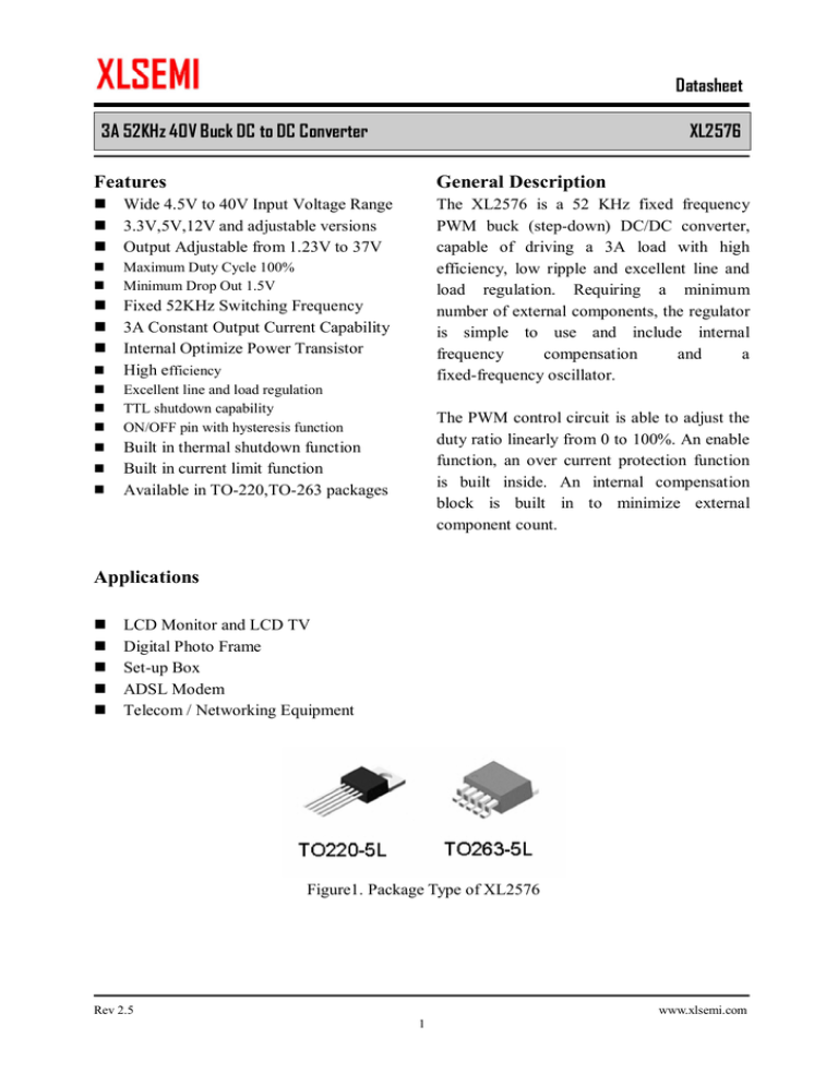
Datasheet 3A 52KHz 40V Buck DC to DC Converter XL2576 Features General Description Wide 4.5V to 40V Input Voltage Range 3.3V,5V,12V and adjustable versions Output Adjustable from 1.23V to 37V Maximum Duty Cycle 100% Minimum Drop Out 1.5V Fixed 52KHz Switching Frequency 3A Constant Output Current Capability Internal Optimize Power Transistor High efficiency The XL2576 is a 52 KHz fixed frequency PWM buck (step-down) DC/DC converter, capable of driving a 3A load with high efficiency, low ripple and excellent line and load regulation. Requiring a minimum number of external components, the regulator is simple to use and include internal frequency compensation and a fixed-frequency oscillator. Excellent line and load regulation TTL shutdown capability ON/OFF pin with hysteresis function The PWM control circuit is able to adjust the duty ratio linearly from 0 to 100%. An enable function, an over current protection function is built inside. An internal compensation block is built in to minimize external component count. Built in thermal shutdown function Built in current limit function Available in TO-220,TO-263 packages Applications LCD Monitor and LCD TV Digital Photo Frame Set-up Box ADSL Modem Telecom / Networking Equipment Figure1. Package Type of XL2576 Rev 2.5 www.xlsemi.com 1 Datasheet 3A 52KHz 40V Buck DC to DC Converter XL2576 Pin Configurations Figure2. Pin Configuration of XL2576 (Top View) Table 1 Pin Description Pin Number 1 2 3 4 5 Pin Name Description Supply Voltage Input Pin. XL2576 operates from a 4.5V to VIN 40V DC voltage. Bypass Vin to GND with a suitably large capacitor to eliminate noise on the input. Power Switch Output Pin (SW). Output is the switch node that OUTPUT supplies power to the output. Ground Pin. Care must be taken in layout. This pin should be placed outside of the Schottky Diode to output capacitor GND ground path to prevent switching current spikes from inducing voltage noise into XL2576. Feedback Pin (FB). Through an external resistor divider FEEDBACK network, Feedback senses the output voltage and regulates it. The feedback threshold voltage is 1.23V. Enable Pin. Drive ON/OFF pin low to turn on the device, drive ON/OFF it high to turn it off. Floating is default low. Rev 2.5 www.xlsemi.com 2 Datasheet 3A 52KHz 40V Buck DC to DC Converter XL2576 Function Block Figure3. Function Block Diagram of XL2576 Typical Application Circuit FEEDBACK 4 VIN OUTPUT 1 XL2576-5.0 2 3 5 GND ON/OFF +12V CIN 470uf 35V C1 105 L1 100uh/3A 5V/3A COUT D1 330uf 35V 1N5820 OFF ON LOAD Figure4. XL2576 Typical Application Circuit 12V-5V/3A Rev 2.5 www.xlsemi.com 3 Datasheet 3A 52KHz 40V Buck DC to DC Converter XL2576 Ordering Information E1 XL2576 E1: Lead Free Circuit Type Package Version ADJ: Adjust 3.3: 3.3V 5.0: 5V 12: 12V S: TO263-5L T: TO220-5L Package Temperature Range TO220-5L -40oC ~ 85oC TO263-5L -40oC ~ 85oC Marking ID Lead Free XL2576T-ADJE1 XL2576T-3.3E1 XL2576T-5.0E1 XL2576T-12E1 XL2576S-ADJE1 XL2576S-3.3E1 XL2576S-5.0E1 XL2576S-12E1 Packing Type Supplied As Tube Tube Tube Tube 800 Units on Tape & Reel 800 Units on Tape & Reel 800 Units on Tape & Reel 800 Units on Tape & Reel XLSEMI Pb-free products, as designated with “E1” suffix in the par number, are RoHS compliant. Rev 2.5 www.xlsemi.com 4 Datasheet 3A 52KHz 40V Buck DC to DC Converter XL2576 Absolute Maximum Ratings(Note1) Parameter Input Voltage Feedback Pin Voltage ON/OFF Pin Voltage Output Switch Pin Voltage Power Dissipation Thermal Resistance (TO220 & TO263) (Junction to Ambient, No Heatsink, Free Air) Operating Junction Temperature Storage Temperature Lead Temperature (Soldering, 10 sec) ESD (HBM) Symbol Vin VFB VON/OFF VOutput PD Value -0.3 to 45 -0.3 to Vin -0.3 to Vin -0.3 to Vin Internally limited Unit V V V V mW RJA 30 ºC/W TJ TSTG TLEAD -40 to 125 -65 to 150 260 >2000 ºC ºC ºC V Note1: Stresses greater than those listed under Maximum Ratings may cause permanent damage to the device. This is a stress rating only and functional operation of the device at these or any other conditions above those indicated in the operation is not implied. Exposure to absolute maximum rating conditions for extended periods may affect reliability. Rev 2.5 www.xlsemi.com 5 Datasheet 3A 52KHz 40V Buck DC to DC Converter XL2576 XL2576-3.3 Electrical Characteristics Ta = 25℃;unless otherwise specified. Symbol Parameter Test Condition Min. Typ. Max. Unit 3.168 3.3 3.432 V - 75 - % Min. Typ. Max. Unit 4.8 5 5.2 V - 78 - % Min. Typ. Max. Unit 11.52 12 12.48 V - 92 - % Min. Typ. Max. Unit 1.193 1.23 1.267 V - 73 - % System parameters test circuit figure6 VOUT Efficiency Output Voltage ŋ Vin = 4.75V to 40V Iload=0.2A to 3A Vin=12V ,Vout=3.3V Iout=3A XL2576-5.0 Electrical Characteristics Ta = 25℃;unless otherwise specified. Symbol Test Condition Parameter System parameters test circuit figure7 VOUT Efficiency Output Voltage ŋ Vin = 7V to 40V Iload=0.2A to 3A Vin=12V ,Vout=5V Iout=3A XL2576-12 Electrical Characteristics Ta = 25℃;unless otherwise specified. Symbol Parameter Test Condition System parameters test circuit figure5 VOUT Efficiency Output Voltage ŋ Vin = 15V to 40V Iload=0.2A to 2A Vin=24V ,Vout=12V Iout=2A XL2576-ADJ Electrical Characteristics Ta = 25℃;unless otherwise specified. Symbol Parameter Test Condition System parameters test circuit figure8 VOUT Efficiency Output Voltage ŋ Vin = 4.5V to 40V Iload=0.2A to 3A Vin=12V ,Vout=3V Iout=3A Rev 2.5 www.xlsemi.com 6 Datasheet 3A 52KHz 40V Buck DC to DC Converter XL2576 Electrical Characteristics (DC Parameters) Vin = 12V for the 3.3V,5V,and Adjustable versions and Vin=24V for the 12V version, GND=0V, Vin & GND parallel connect a 220uf/50V capacitor; Iout=500mA, Ta = 25℃; the others floating unless otherwise specified. Parameters Symbol Input operation voltage Test Condition Vin Min. Typ. 4.5 Max. Unit 40 V Shutdown Supply Current ISTBY VON/OFF=5V 80 200 uA Quiescent Supply Current Iq VON/OFF =0V, VFB =Vin 2 10 mA 40 52 64 Khz 3.6 4.8 6.9 A Oscillator Frequency Fosc Switch Current Limit IL VFB =0 VON/OFF High (Regulator OFF) Low (Regulator ON) 1.4 0.8 IH VON/OFF =2.5V (OFF) 5 15 uA IL VON/OFF =0.5V (ON) 0.2 5 uA VCE VFB=0V Iout=3A 1.3 1.5 V DMAX VFB=0V 100 ON/OFF Pin Threshold ON/OFF Pin Leakage Current Input Output Saturation Voltage Max. Duty Cycle Rev 2.5 V % www.xlsemi.com 7 Datasheet 3A 52KHz 40V Buck DC to DC Converter XL2576 Test Circuit and Layout guidelines Figure5. Standard Test Circuits and Layout Guides Select R1 to be approximately 1K, use a 1% resistor for best stability. C1 and CFF are optional; in order to increase stability and reduce the input power line noise, CIN and C1 must be placed near to PIN1 and PIN3; For output voltages greater than approximately 10V, an additional capacitor CFF is required. The compensation capacitor is typically between 100 pf and 33 nf, and is wired in parallel with the output voltage setting resistor, R2. It provides additional stability for high output voltage, low input-output voltages, and/or very low ESR output capacitors, such as solid tantalum capacitors. CFF=1/(31*1000*R2); This capacitor type can be ceramic, plastic, silver mica, etc. (Because of the unstable characteristics of ceramic capacitors made with Z5U material, they are not recommended.) Rev 2.5 www.xlsemi.com 8 Datasheet 3A 52KHz 40V Buck DC to DC Converter XL2576 XL2576 Series Buck Regulator Design Procedure (Fixed Output) Conditions Output Voltage (V) 3.3 Load Current (A) 3 5 3 Max Input Voltage (V) Inductor (L1) Inductance (uh) 5 10 20 40 7 9 15 40 47 68 100 150 47 68 100 150 Output Capacitor (COUT) Through Hole Electrolytic Panasonic Nichicon HFQ Series PL Series (uf/V) (uf/V) 470/25 560/16 560/35 560/35 680/35 680/35 560/35 470/35 470/25 560/16 560/25 560/25 330/35 330/35 330/35 270/35 Rev 2.5 Surface Mount Tantalum AVX TPS Sprague Series 595D Series (uf/V) (uf/V) 330/6.3 390/6.3 330/6.3 390/6.3 330/6.3 390/6.3 330/6.3 390/6.3 220/10 330/10 220/10 330/10 220/10 330/10 220/10 330/10 www.xlsemi.com 9 Datasheet 3A 52KHz 40V Buck DC to DC Converter XL2576 XL2576 Series Buck Regulator Design Procedure (Adjustable Output) Output Voltage (V) 2 4 6 9 12 15 24 28 Through Hole Output Electrolytic Panasonic Nichicon Feedforward HFQ Series PL Series Capacitor (uf/V) (uf/V) 820/35 820/35 33nf 560/35 470/35 10nf 470/25 470/35 3.3nf 330/25 330/25 1.5nf 330/25 330/25 1nf 220/25 220/35 680pf 220/35 150/35 560pf 100/50 100/50 390pf Surface Mount Output Capacitor AVX TPS Sprague Feedforward Series 595D Series Capacitor (uf/V) (uf/V) 330/6.3 470/4 33nf 330/6.3 390/6.3 10nf 220/10 330/10 3.3nf 100/16 180/16 1.5nf 100/16 180/16 1nf 68/20 120/20 680pf 33/25 33/25 220pf 10/35 15/50 220pf Schottky Diode Selection Table Current 1A 3A Surface Through VR (The same as system maximum input voltage) Mount Hole 20V 30V 40V 50V 1N5817 1N5818 1N5819 √ √ 1N5820 1N5821 1N5822 √ MBR320 MBR330 MBR340 MBR350 MBR360 SK32 SK33 SK34 SK36 30WQ03 30WQ04 30WQ05 31DQ03 31DQ04 31DQ05 SR305 SR306 √ √ √ 5A √ 60V SK35 √ SR302 SR303 SR304 √ 1N5823 1N5824 1N5825 √ SR502 SR503 SR504 SR505 SR506 √ SB520 SB530 SB540 SB550 SB560 50WQ03 50WQ04 50WQ05 Rev 2.5 www.xlsemi.com 10 Datasheet 3A 52KHz 40V Buck DC to DC Converter XL2576 Typical System Application for 3.3V Version FEEDBACK 4 VIN OUTPUT 1 XL2576-3.3 2 3 5 GND ON/OFF +12V CIN 470uf 35V C1 105 L1 100uh/3A 3.3V/3A COUT D1 470uf 35V 1N5820 OFF ON LOAD Figure6. XL2576-3.3 System Parameters Test Circuit Typical System Application for 5V Version FEEDBACK 4 VIN OUTPUT 1 XL2576-5.0 2 3 5 GND ON/OFF +12V CIN 470uf 35V C1 105 L1 100uh/3A 5V/3A COUT D1 330uf 35V 1N5820 OFF ON LOAD Figure7. XL2576-5.0 System Parameters Test Circuit Rev 2.5 www.xlsemi.com 11 Datasheet 3A 52KHz 40V Buck DC to DC Converter XL2576 Typical System Application for ADJ Version CFF 10n R1 1K R2 3.1K FEEDBACK 4 VIN OUTPUT 1 XL2576-ADJ 2 3 5 GND ON/OFF +24V CIN 470uf 50V C1 105 L1 150uh/3A 5V/3A COUT D1 470uf 35V 1N5821 OFF ON LOAD VOUT=1.23*(1+R2/R1) Figure8. XL2576-ADJ System Parameters Test Circuit Rev 2.5 www.xlsemi.com 12 Datasheet 3A 52KHz 40V Buck DC to DC Converter XL2576 Package Information (1) TO220-5L Rev 2.5 www.xlsemi.com 13 Datasheet 3A 52KHz 40V Buck DC to DC Converter XL2576 Package Information (2) TO263-5L Rev 2.5 www.xlsemi.com 14


