A Novel Architecture for Current-steering Digital to
Analog Converters
Ms. Maitry Upraity, Mr. Chetan Parikh
Dhirubhai Ambhani Insititute of Information &
Communication Technology, Gandhinagar,
Gujarat, India.
maitryupraity@gmail.com,
chetan_parikh@daiict.ac.in
Ms. Pallavi G. Darji
Department of Electronics & Communication
Dharmsinh Desai University,
College Road, Nadiad-387 001,
Gujarat, India.
paldarji@yahoo.co.in
Abstract — This paper presents a novel Current Steering
Digital to Analog Converter architecture to reduce area as well as
power dissipation. The current cells of conventional binary
weighted architecture require larger size of transistors for MSBs.
In this paper, same sized current cell transistors for MSBs as that
of LSBs and a current mirror circuit is used between the load
and MSBs to provide necessary higher current. Here, 6-bit CSDAC is simulated. The area of this proposed CS-DAC has
decreased by about 12% and power dissipation by about 50% in
comparison with a conventional Binary architecture.
Keywords—data converters, digital-to-analog,
steering, current mirroring,cascode
I.
N
Inputs
Mx M y
Vin
Vbias2
VDD
Differential
switching
Transistors
N=2n-1
RL
Vout
Vbias1
Current Mirror
Transistor with
current source
Cascode
Transistors
N=2n-1
Current source
Transistors
N=2n-1
Vin
Switching
Transistor
Cascode
Transistor
Current
Source
Figure 2 Current cell with cascode transistor and switching transistor
In this paper, design of a 6-bit Current Steering DAC has
been reported. The technology used for the design is 180nm
CMOS process. Larger sizes of current cell transistors at
MSBs are avoided in this architecture by using Current mirror
circuit.
The paper is organized as follows. A review of the
conventional architecture in given section II, the proposed
architecture and its design considerations is described in
section III. Simulation results are given in section IV followed
by the conclusions in section V
Vout
Regulated
Cascode Bias
Circuit
Iout
Iout
current
Digital to analog converters required by digital signal
processors, medical instruments, wireless communication and
other various processing equipment has proved to be a
continuous challenge for the analog designers to improve and
develop new DAC architectures. Current steering DAC is
most popular due to its high speed, high resolution and small
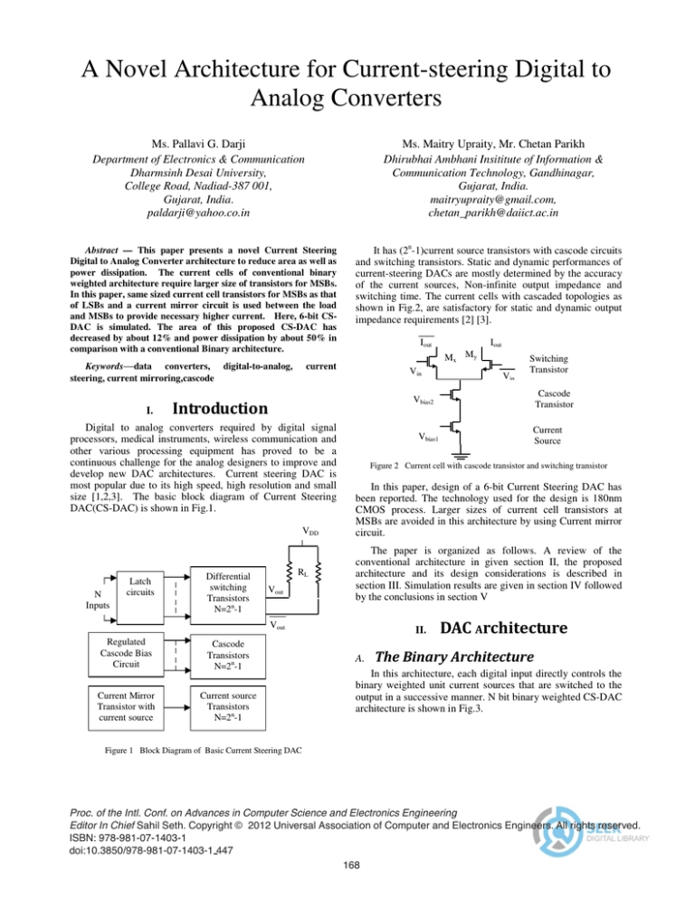
size [1,2,3]. The basic block diagram of Current Steering
DAC(CS-DAC) is shown in Fig.1.
Latch
circuits
It has (2n-1)current source transistors with cascode circuits
and switching transistors. Static and dynamic performances of
current-steering DACs are mostly determined by the accuracy
of the current sources, Non-infinite output impedance and
switching time. The current cells with cascaded topologies as
shown in Fig.2, are satisfactory for static and dynamic output
impedance requirements [2] [3].
II.
A.
In this architecture, each digital input directly controls the
binary weighted unit current sources that are switched to the
output in a successive manner. N bit binary weighted CS-DAC
architecture is shown in Fig.3.
Figure 1 Block Diagram of Basic Current Steering DAC
Proc. of the Intl. Conf. on Advances in Computer Science and Electronics Engineering
Editor In Chief Sahil Seth. Copyright © 2012 Universal Association of Computer and Electronics Engineers. All rights reserved.
ISBN: 978-981-07-1403-1
doi:10.3850/978-981-07-1403-1 447
168
Proc. of the Intl. Conf. on Advances in Computer Science and Electronics Engineering
VDD
changing), reduces the total harmonic distortion and increases
the linearity of the converter [1].
RL
III.
bN
2N-1ILSB
For higher resolution, Binary weighted CS-DAC require
larger size of current source and segmented CS-DAC
architecture consumes more die area [4,5]. In order to
compensate this recede, a new architecture is proposed. In this
design, current mirror circuit for MSBs is used instead of Unit
Elements, as shown in Fig. 5.
b1
bN-1
2N-2ILSB
ILSB
The proposed DAC is based on the current mirror circuit
concept, where the width of MSBs current source transistors is
kept same as the width of LSBs. The Block diagram of
proposed CS-DAC is as shown in Fig. 6.
Figure 3 N-bit Binary Weighted CS-DAC
This architecture is implemented on a small silicon area
and it minimizes the digital power consumption. However, the
most significant bits (MSB) in this architecture control large
currents that are affected by mismatch errors. A large DNL
error may occur when switching on the MSB and all the other
bits off, which leads to a severe degradation of the static
performance for this architecture [2].
B.
Here, two current mirror circuits are employed between the
load and current source transistor. PMOS current mirror
circuit is used as a multiplier for higher MSBs instead of
NMOS, as the amount of current mismatch error is more in
NMOS[2] because of the higher mobility of electrons.
Cascode transistor with mirror transistor helps to improve
linearity of DAC[6]. Use of regulated cascode bias circuit is
as shown in Fig. 7. Regulated cascade circuit has an added
advantage of providing high impedance and high swing
compared to other cascode circuits [8]. Due to the feedback
mechanism, output voltage variation keeps current source
transistor (T1) in saturation. Desired load current and
equivalent analog output voltage across the load is achieved
with this proposed architecture.
In the unary architecture, the current source array consists
of (2N − 1) unity current sources that can be accessed
separately. The digital input code has to be converted to a
decimal code that determines the number of current sources to
be switched to the output. Binary to unary decoder is required
for this architecture. This decoder consumes a lot of silicon
area and has large power consumption, thereby offering a
good DNL specification. Only one extra unity current source
needs to be switched to the output when the digital input value
is increased by one [2].
C.
2I
I
2I
I
In order to obtain architecture with a good DNL
specification having an acceptable power and a minimum area,
a combination of the previous two architectures, known as
Segmented architecture, is chosen. This architecture is widely
used in high-speed and high-accuracy digital-to-analog
converters (DAC’s) [1], [4]–[7]. Fig.4 shows a segmented
current steering DAC (CS DAC) architecture, in which the
least significant bits (LSB’s) are realized using a binaryweighted array and the most significant bits (MSB’s) are
implemented with an unary array(thermometer decoded) .
4I
Figure 5 Basic Concept of use of Current Mirror Circuit for 2-bit MSBs in 4bit CS-DAC.
VDD
LSB
MSB
Unit Element
Current Multiplier
Circuit
(PMOS & NMOS)
Binary Weighted
Binary Weighted
2-bit CS-DAC
Figure 4 Segmented Architecture
Load
Binary Weighted
4-bit CS-DAC
Figure 6 Block Diagram of Proposed CS-DAC
Increasing the number of thermometry bits guarantees the
monotonicity, reduces the glitch energy (caused by timing
mismatch error of the switches while the input code is
169
Proc. of the Intl. Conf. on Advances in Computer Science and Electronics Engineering
Vo
Ii
T1
T3
Vi
T2
Figure 7 Regulated Cascode Circuit
IV.
Ƭ
. The 6-bit current steering DAC is simulated on LTSpice
using 180nm technology. The power consumption of the
proposed DAC is about 0.87mW at 3V power supply. The
core size of the proposed DAC is about 0.26mm2. Thus the
area of the proposed DAC is smaller by 12% than that of
conventional DAC and power dissipation is reducing by 50%.
Figure 9 DNL and INL of 6-bit Proposed Current Mirroring CS-DAC
The Proposed CS-DAC has a monotonic behavior. There is
an initial rising time due to current mirror circuit present
across the load. To avoid this, extra switches are used
between current mirror circuit and load. Fig. 8 shows DAC
output with glitch energy of 14nS.V Extra switches are
responsible for this larger glitch energy.
The maximum glitch energy is observed at transition from
011111->100000. Fig. 11 shows comparison of this glitch
with binary weighted CS-DAC, which is 20% higher
compared to binary weighted CS-DAC.
The 6-bit Current Mirroring CS-DAC Real as well as
differential output is shown in Fig. 8.
Figure 10 Glitch Energy (at 011111-> 100000) in (a) Binary Weighted (b)
Current Mirroring CS-DAC
V.
From this work, it can be concluded that the incorporation
of current mirror circuit in the design of analog circuits helps
to avoid larger width of current source transistors at MSBs to
get higher current. Further, the area and power dissipation of
the proposed DAC architecture is less as compare to the other
DAC architectures. The performance of the circuit is
summarized in Table. 1.
Figure 8 Real as well as Differential Analog output of 6 bit proposed Current
Mirroring CS-DAC
The measured DNL and INL errors are less than 0.15 LSB
as shown in Fig. 10.
170
Proc. of the Intl. Conf. on Advances in Computer Science and Electronics Engineering
TABLE I.
PERFORMANCE COMPARISON
Performance
Parameter
Binary Weighted
CS-DAC
Proposed
Design
Resolution
6-bit
6-bit
Technology
180nm
180nm
DNL
0.13LSB
0.13LSB
INL
0.13LSB
0.13LSB
Glitch Energy
12nsV
14nsV
Power Supply
3v
3V
Power Dissipation
1.9mW
[3]
[4]
[5]
[6]
Chip Area
(DAC Core)
0.87mW
2
0.292mm
[7]
0.262mm2
[8]
ZĞĨĞƌĞŶĐĞƐ
[1]
[2]
[9]
Zhi-Yuan Cui, Hua-Lan Piao, and Nam-Soo Kim, “A 10-bit Currentsteering DAC in 0.35-μm CMOS Process” Transactions On Electrical
And Electronic Materials Vol. 10, No. 2, April 25, 2009
Mircea Tomoroga, Lucian Jurca, “Study of Matching Errors in Unit
Element Approach of Current-Steering Segmented DAC Design.” 6th
[10]
[11]
171
WSEAS International Confeence on System Science and Simulation in
Engineering, 2007
Eulalia Valestrieri, “Some Critical Notes on DAC Time Domain
Specifications” Instrumentation and Measurement “Technology
Conference, Italy, April-2006.
Jurgen Deveugele, Michiel S.J.Steyaert, “A 10-bit 250-MSPS BinaryWeighted Current-Steering DAC” IEEE Journal of Solid-State Circuits,
Vol-41, No.2 Feb.-2006.
J. Huynh, B. Ngo, M. Pham and L.He, “Design of a 10-bit TSMC
0.25um CMOS Digital to Analog Converter” Proceedings of the 6th
international Symposium on Quality Electronic Design-2005
Patrick G. Drennan and Colin C. McAndrew, “Understanding MOSFET
Mismatch for Analog Design” IEEE Journal Of Solid-State Circuits,
Vol. 38, No. 3, March 2003
J Jacob Wikner, “Studies on CMOS Digital-to-Analog Converters”,
Dissertation No. 667, Linköping Studies in Science and Technology,
2001.
T. Loeliger , W. Guggenbhl, ” Cascode Circuits For Low-Voltage And
Low-Current Applications” IEEE Journal of Solid-State Circuits, vol.25,
,Feb.1991.
C.-H. Lin, K. Bull,“A 10 b, 500 M sample/s CMOS DAC in 0.6 mm2,”
IEEE J. Solid-State Circuits, vol. 33, no. 12, pp. 1948–1958, Dec. 1998
T.Miki et al., “An 80-MHz 8-bit CMOS D/A converter”, IEEE JSSC,
vol. 21, no.6, pp. 983-988, Dec. 1985.
Gray, Hurt, Lewis, Meyer “Analysis and Design of Analog Integrated
Circuits”,book

