ISSN: 2278 – 909X
International Journal of Advanced Research in Electronics and Communication Engineering (IJARECE)
Volume 5, Issue 3, March 2016
CURRENT STEERING BASED SIXTEEN BIT
DIGITAL TO ANALOG CONVERTER USING
8T OPERATIONAL AMPLIFIER
S.K.Kabilesh,
M.E., Embedded System Technologies
Sri Shakthi Institute of Engineering and Technology
Coimbatore.
was a segmented one, which consists of binary weighted
current cells or thermometer decoded cells. However only
ABSTRACT
In electronics, a Digital-to-Analog converter (DAC)
is a device that converts digital signal to an analog signal. In
our project, we had proposed a 16-bit, 5MHz current-steering
digital-to-analog converter for system-on-a-chip (SOC)
applications. There are several DAC architecture, they are
Binary weighted DAC, R-2R ladder DAC, Delta-sigma DAC,
segmented DAC. In our project we used segmented DAC
architecture. Segmented design is a hybrid design between
binary weighted and thermometer decoded logic. We adapt
the segmented architecture to obtain better performances on
Glitch energy, and monotonicity. Segmentation is needed to
minimize glitches and nonlinearity in the system outputs.
Current steering circuit is used for summing the signals from
segmented architecture. The fact that current steering
topology used for instead of R-2R topology gives good INL as
well as DNL.8T op-amp technology is used. Based on the
CMOS 0.18 µm technology, we use TSPICE to simulate the
proposed DAC. It has four blocks, Register, decoder, current
cell array and opamp that produce analog voltage in form of
output .It mainly used for Protocol Communication.
Keywords— Current steering , Master slave
register, Decoder, Current Cell Matrix, Current Cell Array,
8T opamp.
one or two bits are segmented.Glitching is not significantly
reduced.Also,high resolution DAC are known to occupy
less area on the die compared to non-segmented
counterpart.
III. BLOCK DIAGRAM
Current cell:-The current cell consists of Digital
and analog part. The digital part consists of the decoding
logic with the clocked pass transistors to control switches
and analog part consisting of cascaded current sources with
the differential switch pair M1 and M2.The output current
of all cells are summed and total current will be supplied to
load resistors R1 and R2 converting into the output voltage.
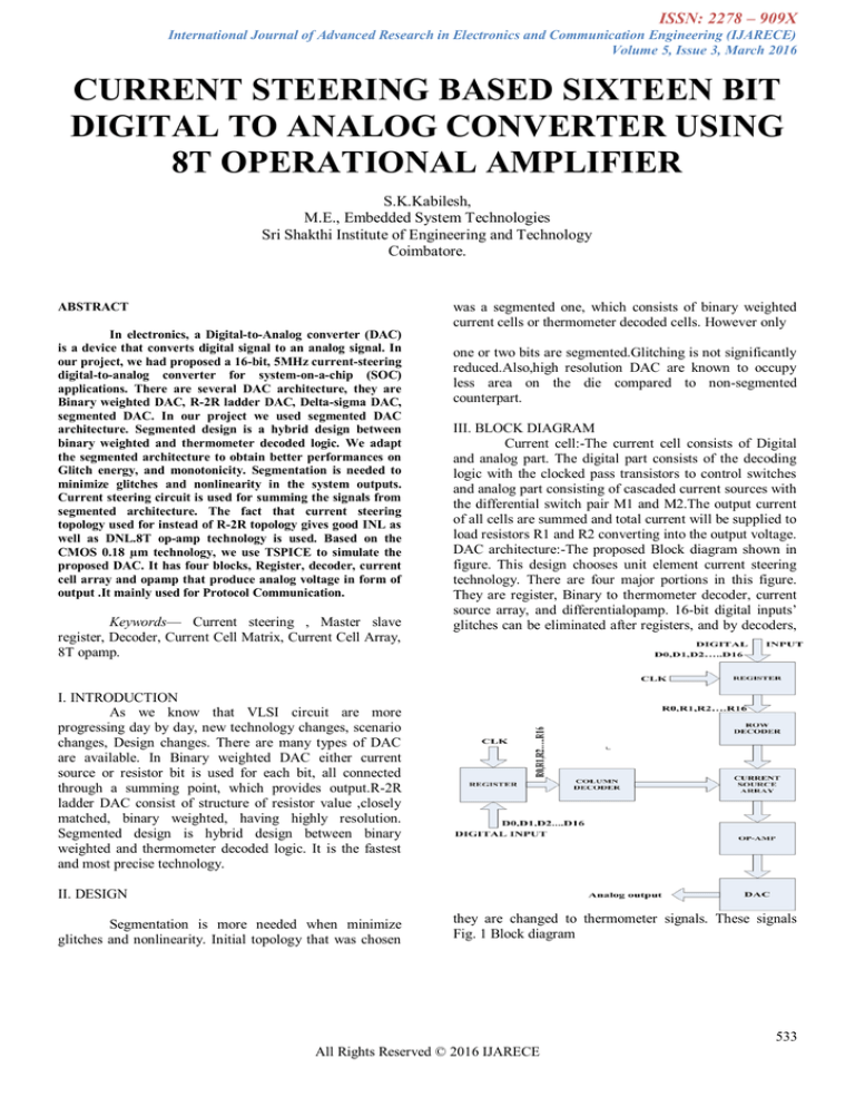
DAC architecture:-The proposed Block diagram shown in
figure. This design chooses unit element current steering
technology. There are four major portions in this figure.
They are register, Binary to thermometer decoder, current
source array, and differentialopamp. 16-bit digital inputs’
glitches can be eliminated after registers, and by decoders,
I. INTRODUCTION
As we know that VLSI circuit are more
progressing day by day, new technology changes, scenario
changes, Design changes. There are many types of DAC
are available. In Binary weighted DAC either current
source or resistor bit is used for each bit, all connected
through a summing point, which provides output.R-2R
ladder DAC consist of structure of resistor value ,closely
matched, binary weighted, having highly resolution.
Segmented design is hybrid design between binary
weighted and thermometer decoded logic. It is the fastest
and most precise technology.
II. DESIGN
Segmentation is more needed when minimize
glitches and nonlinearity. Initial topology that was chosen
they are changed to thermometer signals. These signals
Fig. 1 Block diagram
533
All Rights Reserved © 2016 IJARECE
ISSN: 2278 – 909X
International Journal of Advanced Research in Electronics and Communication Engineering (IJARECE)
Volume 5, Issue 3, March 2016
Perform as controlled codes to determine how many
current cells are on/ off. Finally, in the last stage, the
difference between the inputs of differential amplifiers can
be amplified and serve as the analog output. The Block
diagram is shown above.
REGISTER
It transfers digital bits to next block i.e.
Decoder. Here, there are many types of analog and digital
registers. Without the DAC register, the output of the DAC
Register is used as an elementary component that
is used to store the data. Basically it works as a storage
element, where input bit is stored. It depends on the type of
DAC, like in 8 bit DAC it is of 8 bit, in case of 16 bit, it is
of 16 bit. Here we are using 16 bit register. After all it is
used
to
increase
resolution.
Binary
0000
0001
0010
0011
0100
0101
0110
0111
1000
1001
1010
Thermometer decoder
000 0000 0000 0000
000 0000 0000 0001
000 0000 0000 0011
000 0000 0000 0111
000 0000 0000 1111
000 0000 0001 1111
000 0000 0011 1111
000 0000 0111 1111
000 0000 1111 1111
000 0001 1111 1111
000 0011 1111 1111
TABLE.1 TRUTH TABLE
Fig. 2 Master slave register
Would change immediately with any changes on the
external input bus, due to the real-time feeding of the
analog circuitry. The DAC register acts like a flip-flop. It is
like the operation of Master Slave register.
DECODER
A decoder is a device which does the reverse
operation of an encoder, undoing the encoding so that the
original information can be retrieved. The same method
used to encode is usually just reversed in order to decode.
It is a combinational circuit that converts binary
information from n input lines to a maximum of 2n unique
output lines. In digital electronics, a decoder can take the
form of a multiple-input, multiple-output logic circuit that
converts coded inputs into coded outputs, where the input
and output codes are different.
For example, n to2 n decoders, binary-coded
decimal decoders. Enable inputs must be on for the decoder
to function, otherwise its outputs assume a single
"disabled" output code word.
It is quite difficult to convert the digital to analog
signal rather than analog to digital. So to perform this we
use one technique or configuration called Binary to
Thermometer Decoder logic. In this technique we use row
or column decoder as an elementary block. There are some
important points. To design this we ensure that only one bit
changes per state. Multi bit changes simultaneously causes
big glitches. Use of Row and column decoder keeps layout
compact. In this architecture row decoder, column decoder,
array cell and multiple gates are used. The given
observation table or truth table is shown below.
4.4.3 CURRENT CELL ARRAY
Current cell array is used to perform sum of all
analog currents .It is basically combination of blocks. In
current cell high impedance current mirror will be needed
to reduce the currents, sensitivity to the output voltage and
reduce current glitches that might occur because of change
fig.3 current cell array
In output voltage. It is basically used for amplification
purpose
4.4.4 8T OPERATIONAL AMPLIFIER
An operational amplifier (op-amp) is a DCcoupled high-gain electronic voltage amplifier with a
differential input and, usually, a single-ended output. In
this configuration, an op-amp produces an output potential
534
All Rights Reserved © 2016 IJARECE
ISSN: 2278 – 909X
International Journal of Advanced Research in Electronics and Communication Engineering (IJARECE)
Volume 5, Issue 3, March 2016
(relative to circuit ground) that is typically hundreds of
thousands of times larger than the potential difference
between its input terminals. Operational amplifiers had
voltage at the output. This circuit also implements Miller
compensation capacitor to achieve stable operation when
negative feedback is applied around the OPAMP
RESULT & SIMULATION
POWER ANALYSIS
o
o
o
their origins in analog computers, where they were used to
do mathematical operations in many linear, non-linear and
fig.4 8T operational amplifier
Frequency-dependent circuits. Characteristics of a circuit
using an op-amp are set by external components with little
dependence on temperature changes or manufacturing
variations in the op-amp itself, which makes op-amps
popular building blocks for circuit design. Op-amp is used
as current to voltage converter.
o The voltage gain can be controlled by
externally providing feedback.
o The op-amp can be used in almost any d.c
to 1MHz amplifier and signal processing
applications.
o Output voltage VO=A (V1-V2).
An ideal op-amp is usually considered to have the
following properties:
o
o
o
o
o
Infinite open-loop gain and Power supply
rejection ratio
Infinite voltage range available at the
output
Infinite input impedance and so zero input
current and zero input offset voltage
Zero output impedance
Infinite Common-mode rejection ratio
(CMRR)
An eight-transistor benchmark model for the design of the
OPAMP. It is a classical two-stage CMOS operational
amplifier .The first stage consists of a differential amplifier
converting
the
differential
input
voltage
to
differentialcurrents. These differential currents are applied
to a current mirror load to recover the differential voltage.
The second stage is a common source converting the
second stage input voltage to current. This transistor is
loaded by a current-sink load, which converts the current to
T-Spice tool used for analyzing the average
power, static power and dynamic power.
Static power is power consumed while there is no
circuit activity. For example, the power consumed
by a flip-flop when neither clock nor input have
active inputs. (i.e., all inputs are “static” because
they are fixed at DC levels).
Dynamic power is power consumed while the
inputs are active.
Fig.5 output waveform
ENERGY DELAY PRODUCT
Energy Delay Product (EDP) is to determine
quality of digital gate and measure the energy of gate, we
use the product of power dissipation and square of
propagation delay.
EDP is therefore define as EDP=PD*(tP)2
.
POWER DELAY PRODUCT
Power Delay Product (PDP) is to quantify how
effective, or efficient a digital design technology is in terms
of delay and power, we use the product of the propagation
delay and power dissipation.
PDP is therefore define as PDP=PD*tP .
AREA
Area is the size of the surface occupied by the
circuit. It can be calculated by using length and width of
the transistor.
535
All Rights Reserved © 2016 IJARECE
ISSN: 2278 – 909X
International Journal of Advanced Research in Electronics and Communication Engineering (IJARECE)
Volume 5, Issue 3, March 2016
Area = (number of transistor)*(length)*(width of
the transistor).
PARAMETER
VALUE
Bit
16
Power
6.64w
dynamic power
0.007w
Frequency
5MHZ
PDP
0.18 µJ
EDP
4.5 PJ
Area
0.6 nm2
Asad Abbas Syed (2006)” HIGH ‐SPEED 8‐BIT PIPELINE
CURRENT‐STEERING D/A CONVERTER “”, IJERT.
TABLE.2 output results
CONCLUSION
The 16-bit DAC using current steering technique
was designed promptly which has 16-bit resolution and
simulated with the help of TSPICE. This operates at the
voltage of 1.8v and the clock frequency of 5 MHz This
DAC was designed using CMOS 0.18µm technology. It
consumes 6W power and 0.6nm2 consumption of area.
Glitches were reduced with the help of current steering
technique. Segmented architecture improved the
monotonicity. In near future it may be possible to reduce
the power by using other technology like alpha-latch, sense
amp, etc…. While the DAC is implemented by CNTFET
manufacturing technology, hence there is a chance of
reduction in power.
REFERENCES
VineetTiwari, Prof.SanjeevRajan, Prof.Vivek Baghel, (July2012) “DESIGN OF 8 BIT CURRENT STEERING DAC”, IJERT- vol.1,
issue 5.
Li Xueqing, Fan Hua, Wei Qi, Xu Zhen, Liu Jianan, and Yang
Huazhong (2013) “A 14-BIT 250-MS/S CURRENT-STEERING CMOS
DIGITAL-TO-ANALOG CONVERTER”, Journal of Semiconductors- Vol.
34, No.
Helna Aboobakear, Ramya Jayachandran, (july-2013)
“DESIGN,IMPLEMENTATION & COMPARISON OF 8BIT 100MHZ
CURRENT STEERING DAC’s”, IJERA, vol.3, issue 4.
G.Bertotti, A.Laifi (2012) “AN 8-BIT CURRENT STEERING
DAC”, IEEE.
Fahim Rahman, Asheque Mohammad Zaidit, Nadia Anamt,
Aysha Aktert (2011) “Performance Evaluation of a 32-nm CNT-OPAMP
Design, Characteristic Optimization and Comparison with CMOS
Technology” ICCIT.
Vango Technol.Inc., Hangzhou (2008) “A 12-BIT 150MSAMPLE/S CURRENT STEERING DAC ” IEEE.
Dougles A.Merer, (october-2008) “DIGITAL TO ANALOG
CONVERTER DESIGN”, IEEE student chapter.
536
All Rights Reserved © 2016 IJARECE


