AMMP-6522
7 to 20 GHz GaAs MMIC LNA/IRM Receiver
in SMT Package
Data Sheet
Description
Features
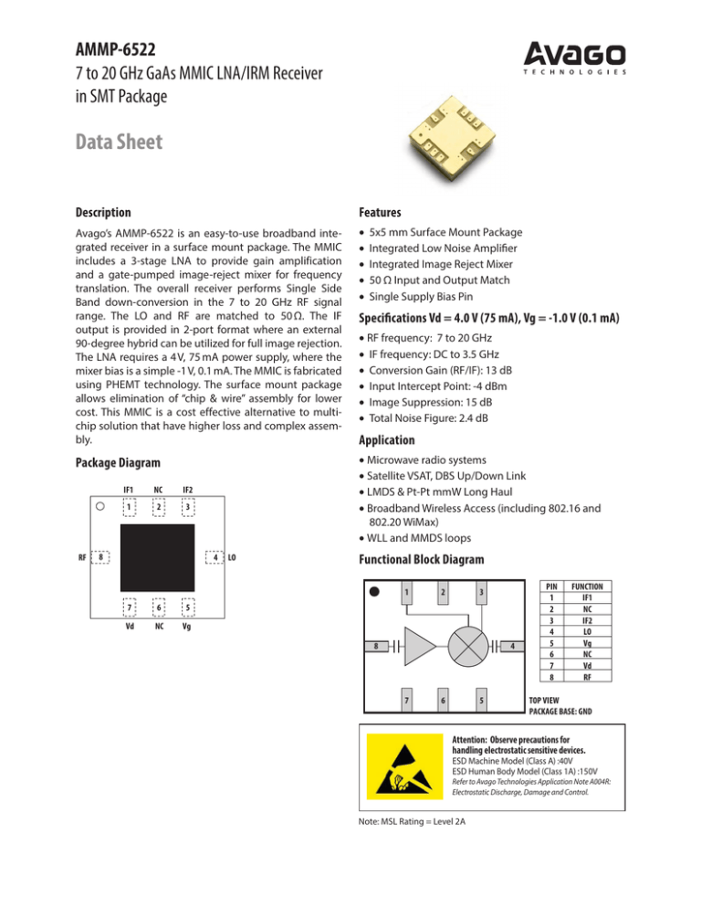
Avago’s AMMP-6522 is an easy-to-use broadband integrated receiver in a surface mount package. The MMIC
includes a 3-stage LNA to provide gain amplification
and a gate-pumped image-reject mixer for frequency
translation. The overall receiver performs Single Side
Band down-conversion in the 7 to 20 GHz RF signal
range. The LO and RF are matched to 50 Ω. The IF
output is provided in 2-port format where an external
90-degree hybrid can be utilized for full image rejection.
The LNA requires a 4 V, 75 mA power supply, where the
mixer bias is a simple -1 V, 0.1 mA. The MMIC is fabricated
using PHEMT technology. The surface mount package
allows elimination of “chip & wire” assembly for lower
cost. This MMIC is a cost effective alternative to multichip solution that have higher loss and complex assembly.
•5x5 mm Surface Mount Package
•Integrated Low Noise Amplifier
•Integrated Image Reject Mixer
•50 Ω Input and Output Match
•Single Supply Bias Pin
Package Diagram
•Microwave radio systems
•Satellite VSAT, DBS Up/Down Link
•LMDS & Pt-Pt mmW Long Haul
•Broadband Wireless Access (including 802.16 and
802.20 WiMax)
•WLL and MMDS loops
RF
IF1
NC
IF2
1
2
3
8
4
LO
Specifications Vd = 4.0 V (75 mA), Vg = -1.0 V (0.1 mA)
•RF frequency: 7 to 20 GHz
•IF frequency: DC to 3.5 GHz
•Conversion Gain (RF/IF): 13 dB
•Input Intercept Point: -4 dBm
•Image Suppression: 15 dB
•Total Noise Figure: 2.4 dB
Application
Functional Block Diagram
1
7
6
5
Vd
NC
Vg
2
3
8
4
7
6
5
PIN
1
2
3
4
5
6
7
8
FUNCTION
IF1
NC
IF2
LO
Vg
NC
Vd
RF
TOP VIEW
PACKAGE BASE: GND
Attention: Observe precautions for
handling electrostatic sensitive devices.
ESD Machine Model (Class A) :40V
ESD Human Body Model (Class 1A) :150V
Refer to Avago Technologies Application Note A004R:
Electrostatic Discharge, Damage and Control.
Note: MSL Rating = Level 2A
Electrical Specifications
1.Small/Large -signal data measured in a fully de-embedded test fixture form TA = 25°C.
2.Pre-assembly into package performance verified 100% on-wafer per AMMC-6522 published specifications.
3.This final package part performance is verified by a functional test correlated to actual performance at one or more
frequencies.
4.Specifications are derived from measurements in a 50 Ω test environment. Aspects of the amplifier performance
may be improved over a more narrow bandwidth by application of additional conjugate, linearity, or low noise
(Гopt) matching.
5.NF is measure on-wafer. Additional bond wires (-0.2nH) at Input could improve NF at some frequencies.
Table 1. RF Electrical Characteristics
TA=25°C, Vd=4.0V, Vg=-1V, Zo=50 Ω, LO=+15dBm, IF=2GHz [1]
RF=8GHz, LO=10GHz
Parameter
Min
Noise Figure into 50 Ω, NF
Typ
Max
2.6
3.3
RF=18GHz, LO=20GHz
Min
Typ
Max
Unit
3
3.3
dB
Conversion Gain, CG
12
13
12
14
dB
Input Third Order Intercept, IIP3
-8
-6
-5
-0.4
dBm
Image Rejection, Sup
15
29
15
30
dB
Comment
Note:
1. All tested parameters are guaranteed with the following measurement accuracy:
RF=8GHz: ±0.6dB for Conversion Gain, ±10dB for IRR, ±0.5dB for NF, ±0.8dBm for IIP3
RF=18GHz: ±1.8dB for Conversion Gain, ±1.6dB for IRR, ±0.6dB for NF, ±1.7dBm for IIP3
Table 2. Recommended Operating Range
1.Ambient operational temperature TA = 25°C unless otherwise noted.
2.Channel-to-backside Thermal Resistance (Tchannel (Tch) = 34°C) as measured using infrared microscopy. Thermal
Resistance at backside temperature (Tb) = 25°C calculated from measured data.
Description
Min.
Drain Supply Current, Id
Typical
Max.
Unit
Comments
75
95
mA
Vd = 4.0 V
Drain Supply Voltage, Vd
3
4
5
V
Gate Supply Voltage, Vg
-1.2
-1.0
-0.8
V
RF Frequency, RFfreq
7
20
GHz
LO Frequency, LOfreq
5
22
GHz
IF Frequency, IFfreq [1]
DC
3.5
GHz
LO Drive Power, LO
+10
+22
dBm
+15
Note:
1. Use IF = DC with caution. Please see “Biasing and Operation” for more details.
2
Ig = 0.1mA
Table 3. Thermal Properties
Parameter
Test Conditions
Value
Thermal Resistance,
qjc
Ambient operational temperature TA = 25°C
Channel-to-backside Thermal Resistance Tchannel(Tch)=34°C
Thermal Resistance at backside temperature Tb=25°C
qjc = 27 °C/W
Absolute Minimum and Maximum Ratings
Table 4. Minimum and Maximum Ratings
Description Pin
Max.
Unit
Drain to Ground Supply Voltage, Vd
5.5
V
Gate to Ground Voltage, Vg
+0.8
V
Drain Current , Id
100
mA
Gate Current, Ig
1
mA
RF CW Input Power, Pin
10
dBm
Channel Temperature, Tch
+150
°C
+150
°C
260
°C
Storage Temperature, Tstg
Maximum Assembly Temperature, Tmax
Min.
-65
Notes:
1. Operation in excess of any one of these conditions may result in permanent damage to this device.
3
Comments
CW
20 second maximum
AMMP-6522 Typical Performance[1,2]
(TA = 25°C, Vd = 4 V, Id = 75 mA, Vg = -1 V, Ig = 0 mA, Zin = Zout = 50 Ω), IF Freq = 2 GHz,
LO Power = +15 dBm unless noted)
20
5
4
LSB
USB
NOISE FIGURE (dB)
CONV GAIN (dB)
10
0
-10
3
2
1
-20
6
8
10
12
14
16
18
0
20
6
8
10
FREQUENCY (GHz)
14
16
18
20
16
18
20
Figure 2. Typical noise figure
Figure 1. Receiver conversion gain
0
5
-10
0
IIP3 (dBm)
RETURN LOSS (dB)
12
FREQUENCY (GHz)
-5
-20
RF
LO
-30
0
10
20
30
40
-10
50
6
8
10
12
14
FREQUENCY (GHz)
FREQUENCY (GHz)
Figure 4. Typical input IP3
Figure 3. Return loss at RF & LO ports
20
0
IIP3 (dBm)
CONV GAIN (dB)
-5
10
LSB
USB
0
-10
-10
-15
-6
-2
2
6
10
14
-20
18
-5
0
5
LO POWER (dBm)
10
15
20
LO POWER (dBm)
Figure 5. Conv gain vs. LO power (RF = 15 GHz)
Figure 6. Input IP3 vs. LO power (RF = 15 GHz)
20
2
0
-2
IIP3 (dBm)
CONV GAIN (dB)
15
10
0
6
8
10
12
14
16
FREQUENCY (GHz)
Figure 7. LSB conversion gain at two IF frequencies
4
-6
IF = 1 GHz
IF = 2 GHz
5
18
-4
IF = 1 GHz
IF = 2 GHz
-8
20
-10
6
8
10
12
14
FREQUENCY (GHz)
Figure 8. Input IP3 at two IF frequencies
16
18
20
AMMP-6522 Typical Performance (cont.)[1,2]
(TA = 25°C, Vd = 4 V, Id = 75 mA, Vg = -1 V, Ig = 0 mA, Zin = Zout = 50 Ω), IF Freq = 2 GHz, LO Power = +15 dBm unless
noted)
18
2
0
INPUT IP3 (dBm)
CONV GAIN (dB)
16
14
Vg = -1.2 V
Vg = -1.1 V
Vg = -1.0 V
Vg = -0.9 V
12
10
6
8
10
12
14
-2
-4
-6
Vg = -1.2 V
Vg = -1.1 V
Vg = -1.0 V
Vg = -0.9 V
-8
16
18
-10
20
6
8
10
FREQUENCY (GHz)
NOISE FIGURE (dB)
CONV GAIN (dB)
20
4
10
4V
3V
5V
5
6
8
10
12
14
16
18
3
2
4V
3V
5V
1
0
20
6
8
10
FREQUENCY (GHz)
12
14
16
18
20
FREQUENCY (GHz)
Figure 11. Receiver conversion gain over Vd
Figure 12. Noise figure over Vd
0
5
-10
0
IIP3 (dBm)
RETURN LOSS (dB)
18
5
15
-20
-5
25C
-40C
85C
0
10
20
30
40
-10
50
4V
3V
5V
6
8
10
FREQUENCY (GHz)
12
14
16
18
20
16
18
20
FREQUENCY (GHz)
Figure 13. Return loss at RF over temperature
Figure 14. Input IP3 over Vd
5
0
25C
-40C
85C
25C
-40C
85C
4
NOISE FIGURE (dB)
LO RETURN LOSS (dB)
16
FREQUENCY (GHz)
20
-30
14
Figure 10. Input IP3 over Vga
Figure 9. Conversion gain over Vg
0
12
-10
-20
3
2
1
-30
0
10
20
30
FREQUENCY (GHz)
Figure 15. Return loss at LO over temperature
40
50
0
6
8
10
12
14
FREQUENCY (GHz)
Figure 16. Noise figure over temperature
Notes:
1. S-parameters are measured with R&D Eval Board as shown in Figure 19. Board and connector effects are included in the data.
2. Noise Figure is measured with R&D Eval Board as shown in Figure 19, and with a 3-dB pad at input. Board and connector losses are already deembeded from the data.
5
Biasing and Operation
The AMMP-6522 is normally biased with a positive
drain supply connected to the Vd pin and a negative
gate voltage connected to the Vg pin through bypass
capacitors as shown in Figure 17. The recommended
drain supply voltage is 4 V and gate bias voltage is -1 V.
The corresponding currents are 75 mA and 0.1 mA respectively. The typical required LO level is +15 dBm and
it should come from a low noise driver to ensure that
overall Front End NF is low.
The image rejection performance is dependent on the
selection of the IF quadrature hybrid. The performance
of the IF hybrid as well as the phase balance and VSWR
of the interface to the AMMP-6522 will affect the overall
front end performance.
The recommended Vg is -1 V. However, depending on
the operating frequency, Vg can be changed to achieve
better performance for that particular frequency.
Please refer to Figures 9 and 10 for how to best select the
appropriate Vg for the intended frequency of operation.
Theoretically IF frequencies can be as low as DC. However,
when direct conversion is used (IF = DC), a so-called
phenomenon DC-offset could occur at the two IF
outputs. In most practical applications, IF should be
more than a few hundreds kHz to avoid DC-offset correction.
Refer the Absolute Maximum Ratings table for allowed
DC and thermal condition.
There is minimal performance degradation if Vdd is
lowered to 3 V or raised to 5 V. If lower current is required, then Vd = 3 V will provide considerably similar RF
performance.
RF
LSB
USB
IF
RF
IF
LO
1000 pF
Vd
1000 pF
Vd
IF1
NC
NC
Vg
IF2
LO
TOP VIEW
LO
+15 dBm
6
IF
1-3.5 GHz
USB
Vg
Figure 17. Application of receiver with IF Balun
LSB
PACKAGE BASE: GND
AMMP-6522 Part Number Ordering Information
Part Number
Devices per Container Container
AMMP-6522-BLKG
10
Antistatic bag
AMMP-6522-TR1G
100
7” Reel
AMMP-6522-TR2G
500
7” Reel
Package Dimension, PCB Layout and Tape and Reel information
Please refer to Avago Technologies Application Note 5520, AMxP-xxxx production Assembly Process (Land Pattern A).
For product information and a complete list of distributors, please go to our website:
www.avagotech.com
Avago, Avago Technologies, and the A logo are trademarks of Avago Technologies in the United States and other countries.
Data subject to change. Copyright © 2005-2013 Avago Technologies. All rights reserved.
AV02-0244EN - July 8, 2013


