SP6644/6645 Evaluation Board Manual
advertisement
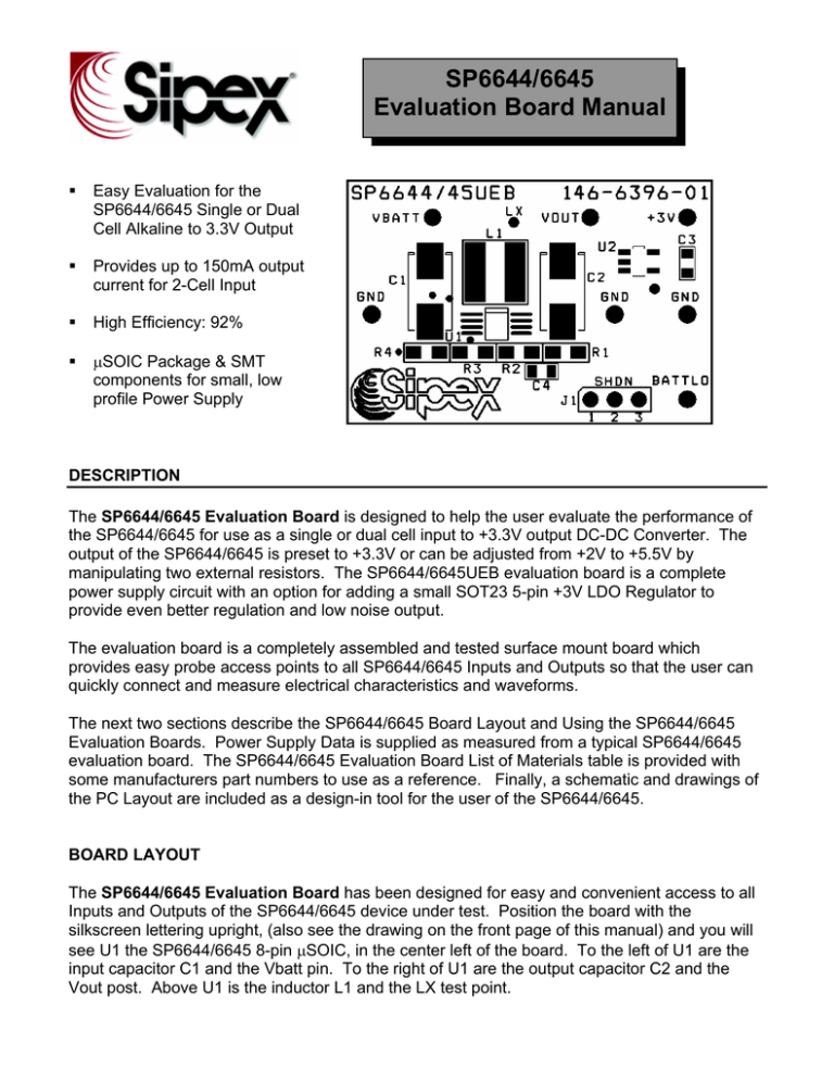
SP6644/6645 Evaluation Board Manual Easy Evaluation for the SP6644/6645 Single or Dual Cell Alkaline to 3.3V Output Provides up to 150mA output current for 2-Cell Input High Efficiency: 92% µSOIC Package & SMT components for small, low profile Power Supply DESCRIPTION The SP6644/6645 Evaluation Board is designed to help the user evaluate the performance of the SP6644/6645 for use as a single or dual cell input to +3.3V output DC-DC Converter. The output of the SP6644/6645 is preset to +3.3V or can be adjusted from +2V to +5.5V by manipulating two external resistors. The SP6644/6645UEB evaluation board is a complete power supply circuit with an option for adding a small SOT23 5-pin +3V LDO Regulator to provide even better regulation and low noise output. The evaluation board is a completely assembled and tested surface mount board which provides easy probe access points to all SP6644/6645 Inputs and Outputs so that the user can quickly connect and measure electrical characteristics and waveforms. The next two sections describe the SP6644/6645 Board Layout and Using the SP6644/6645 Evaluation Boards. Power Supply Data is supplied as measured from a typical SP6644/6645 evaluation board. The SP6644/6645 Evaluation Board List of Materials table is provided with some manufacturers part numbers to use as a reference. Finally, a schematic and drawings of the PC Layout are included as a design-in tool for the user of the SP6644/6645. BOARD LAYOUT The SP6644/6645 Evaluation Board has been designed for easy and convenient access to all Inputs and Outputs of the SP6644/6645 device under test. Position the board with the silkscreen lettering upright, (also see the drawing on the front page of this manual) and you will see U1 the SP6644/6645 8-pin µSOIC, in the center left of the board. To the left of U1 are the input capacitor C1 and the Vbatt pin. To the right of U1 are the output capacitor C2 and the Vout post. Above U1 is the inductor L1 and the LX test point. USING THE EVALUATION BOARD 1) Powering Up the SP6644/6645 Circuit The SP6644/6645 Evaluation Board can be powered from inputs from a +0.8V to +3.3V from 1 or 2 alkaline cells or a power supply. Connect with short leads directly to the “Vbatt” and “Gnd” posts. Monitor the Output Voltage and connect the Load between the “Vout” post and the 2nd “GND” post. 2) Using the J1 Jumper: Enabling the SP6644/6645 Output and using the Shutdown Mode The SP6644/6645 output will be Enabled if the J1 Jumper is in the left or pin 1 to 2 position. If J1 is in the pin 2 to 3 position, the Shutdown pin is brought to GND, which puts the SP6644/6645 in the low quiescent Shutdown Mode. 3) Using the LDO Output The SP6644/6645 output connects to an LDO, the SP6201 ultra low drop-out CMOS regulator which has a 3.0V output at up to 150mA. To evaluate the SP6201 performance with the SP6644/6645 input, connect the load across the +3V post and GND and measure both the SP6644/6645 output and SP6201 output with an oscilloscope configured for AC millivolts. As you can see from figure 8 the output ripple voltage is reduced from 60mV to less than 3mV by the LDO. 4) Using the Rlim Function The peak inductor current, IPEAK, is programmed externally by the RLIM resistor connected between the RLIM pin and GND. The peak inductor current is defined by: IPEAK = 1400/RLIM The SP6644/45 datasheet specifications for RLIM give a range of 2.5 to 9.3K ohms. Using the IPEAK equation above gives an IPEAK range of IPEAK range = 150 to 560mA. The saturation current specified for the inductor needs to be greater then the peak current to avoid saturating the inductor, which would result in a loss in efficiency and could damage the inductor. The SP6644/6645 evaluation board uses a Rlim value of 2.5K to allow the circuit to deliver up to 80mA for 1.3V input and 150mA for 2.6V input. Other values could be selected using the above relationships. POWER SUPPLY DATA The SP6644/6645’s high efficiency is illustrated in figures 1 & 2 which has 90 to 93% efficiency for 2 fully charged alkaline cells. Figure 1 with Rlim of 2.5K can deliver more output current than figure 2 with an Rlim of 5K because it has greater peak current, at a price of reduced efficiency. Line/Load curves in figures 3 & 4 show only 10 to 15mV change in output voltage at rated loads of 80mA for 1-cell and 150mA for 2-cell. The no-load battery current the SP6644/6645 application circuit consumes for different Rlim’s of 2.5K & 5K is illustrated in figure 5. In figure 6 the maximum load current the SP6644/6645 can deliver for different Rlim’s of 2.5K & 5K is illustrated. Load transient response to a 15mA to 150mA output load step is shown in figure 7. Finally, in figure 8, SP6644 output ripple of 60mV is improved with the addition of the SP6201 LDO achieving an output ripple of only 3mV. 2 100 90 90 80 Efficiency (%) Efficiency (%) 100 Vb=1.0V 70 Vb=1.3V Vb=2.0V 60 Vb=2.6V 50 40 1.0 10.0 100.0 Vb=1.0V Vb=1.3V 70 Vb=2.0V 60 Vb=2.6V Vb=3.2V 50 Vb=3.2V 0.1 80 40 1000.0 0.1 1.0 Iload (mA) 10.0 100.0 1000.0 Iload (mA) Figure 1. Efficiency Vs Output Current (Vout = 3.3V) Rlim=2.5K Figure 2. Efficiency Vs Output Current (Vout = 3.3V) Rlim=5K 3.33 3.33 3.32 Vout (V) Vout (V) 3.32 3.31 Vb=1.3V 3.30 Vb=2.6V 3.29 3.31 Vb=1.3V 3.30 Vb=2.6V 3.29 3.28 3.28 3.27 3.27 0 0 20 40 60 80 100 120 140 160 180 200 10 20 30 40 50 60 70 80 90 100 Iload (mA) Iload (mA) Figure 3. Line/Load Rejection Vs Output Current (Vout = 3.3V) Rlim=2.5K Figure 4. Line/Load Rejection Vs Output Current (Vout = 3.3V) Rlim=5K 1000 Max Io (mA) Battery Current (uA) 10000 Rlim=2.5k Rlim=5k 100 10 0.0 1.0 2.0 3.0 4.0 240 220 200 180 160 140 120 100 80 60 40 20 0 Rlim=2.5K Rlim=5K 0.0 Vbatt (V) 1.0 2.0 3.0 4.0 Vbatt (V) Figure 5. No-Load Battery Current Vs Vbatt (Vout = 3.3V) Figure 6. Maximum Load Current Vs Vbatt (Vout = 3.3V) Inductor 0.5A/div SP6201 10mV/div Vout 50mV/div SP6644 20mV/div Vbatt 50mV/div Figure 7. Load Transient Response Rlim=2.5K (Vin = 1.3V,Vout = 3.3V) Figure 8. SP6644 and SP6201 Output Ripple Rlim=2.5K (Vin = 1.3V,Vout = 3.3V, Iout=80mA) 3 FIGURE 9: SP6644/6645UEB COMPONENT PLACEMENT FIGURE 10: SP6644/6645UEB PC LAYOUT TOP SIDE FIGURE 11: SP6644/6645UEB PC LAYOUT BOTTOM SIDE 4 SP6644/6645 EVALUATION BOARD SCHEMATIC +0.88V to +3.3V Input VBATT + GND C1 47uF LX L1 22uH 1 J1 +3.3V VOUT R4 1M 2 3 1 2 BATTLO 3 4 SHDN VBATT BATTLO RLIM SHDN SP6644 U1 VOUT LX GND FB R1 8 7 C4 + OPEN OPEN C2 47uF 6 GND 1 2 3 +3.0V VOUT SP6201 VIN VOUT 5 GND ENABLE RESET_N 4 C3 1uF 5 R3 2.5K R2 100K Probe Access Points for external connection by the user TABLE: SP6644/6645EB LIST OF MATERIALS SP6644/45 Evaluation Board List of Materials Ref. Des. Qty. U1 U2 C1,2 C3 C4 L1 R1 R2 R3 R4 TP J1 1 1 1 2 1 0 1 0 1 1 1 7 1 1 Manufacturer Part Number Sipex Corp. Sipex Corp. Sipex Corp. Sanyo TDK Corp 146-6396-01 SP6644EU or SP6645EU SP6201EM5-3.0 6TPA47M C2012X5R1A105K Open CD43-220 Open ERJ-8ENFJ1003 ERJ-8ENF2491 ERJ-8GEY105 0300-115-01-4727100 PTC36SAAN STC02SYAN Sumida Panasonic Panasonic Panasonic Mill-Max Sullins Sullins Layout Component Size 1"x1.5" SP6644/45 Eval PC Board uSO-8 8-pin uSOIC Step-Up DC/DC Conv SOT23-5 5-pin SOT23 200mA LDO 3.0V Output "C" size Poscap Tant. 6.3V 47uF SM 0.1ohm ESR 805 Ceramic 10V 1uF SM 0.05ohm ESR 805 Open 5x5mm 22uH, 0.68A, 0.38ohm, SM Inductor 1206 Open 1206 100K ohm 1/8W 1% 1206 SM 1206 2.49K ohm 1/8W 1% 1206 SM 1206 1M ohm 1/8W 5% 1206 SM .042 Dia Test Point Female Pin .23x.12 3-Pin Header .2x.1 Shunt Vendor Sipex 978-667-7800 Sipex Sipex Sanyo 978-922-6573 TDK 847-803-6100 Open Sumida 847-956-0666 Open Digi-Key 800-344-4539 800-Digi-Key 800-Digi-Key 800-Digi-Key 800-Digi-Key 800-Digi-Key ORDERING INFORMATION Model Temperature Range Package Type SP6644UEB.................................. -40°C to +85°C...................SP6644 Evaluation Board SP6645UEB.................................. -40°C to +85°C...................SP6645 Evaluation Board SP6644EU.....................................-40°C to +85°C......................................8-pin µSOIC SP6645EU.....................................-40°C to +85°C......................................8-pin µSOIC 5
