AMMC-5024
30 KHz – 40 GHz Traveling Wave Amplifier
Data Sheet
Chip Size:
Chip Size Tolerance:
Chip Thickness:
Pad Dimensions:
2350 x 1050 µm (92.5 x 41.3 mils)
±10 µm (±0.4 mils)
100 ± 10 µm (4 ± 0.4 mils)
80 x 80 µm (2.95 ± 0.4 mils)
Description
Features
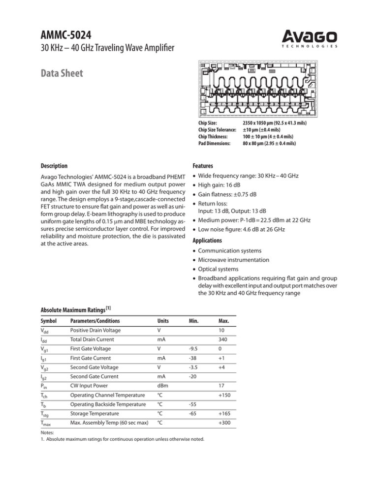
Avago Technologies' AMMC-5024 is a broadband PHEMT
GaAs MMIC TWA designed for medium output power
and high gain over the full 30 KHz to 40 GHz frequency
range. The design employs a 9-stage,cascade-connected
FET structure to ensure flat gain and power as well as uniform group delay. E-beam lithography is used to produce
uniform gate lengths of 0.15 mm and MBE technology assures precise semiconductor layer control. For improved
reliability and moisture protection, the die is passivated
at the active areas.
• Wide frequency range: 30 KHz – 40 GHz
• High gain: 16 dB
• Gain flatness: ±0.75 dB
• Return loss: Input: 13 dB, Output: 13 dB
• Medium power: P-1dB = 22.5 dBm at 22 GHz
• Low noise figure: 4.6 dB at 26 GHz
Applications
• Communication systems
• Microwave instrumentation
• Optical systems
• Broadband applications requiring flat gain and group
delay with excellent input and output port matches over
the 30 KHz and 40 GHz frequency range
Absolute Maximum Ratings [1]
Symbol
Parameters/Conditions
Units
Min.
Max.
Vdd
Positive Drain Voltage
V
10
Idd
Total Drain Current
mA
340
Vg1
First Gate Voltage
V
-9.5
0
Ig1
First Gate Current
mA
-38
+1
Vg2
Second Gate Voltage
V
-3.5
+4
Ig2
Second Gate Current
mA
-20
Pin
CW Input Power
dBm
17
Tch
Operating Channel Temperature
°C
+150
Tb
Operating Backside Temperature
°C
-55
Tstg
Storage Temperature
°C
-65
+165
Tmax
Max. Assembly Temp (60 sec max)
°C
+300
Notes:
1. Absolute maximum ratings for continuous operation unless otherwise noted.
AMMC-5024 DC Specifications/Physical Properties [1]
Symbol
Parameters and Test Conditions
Units
Min.
Typ.
Max.
Idss
Saturated Drain Current (Vdd =7 V, Vg1=0 V, Vg2=open circuit)
mA
265
350
385
Vp
First Gate Pinch-off Voltage (Vdd=7 V, Idd=30 mA, Vg2=open circuit)
V
-8.2
Vg2
Second Gate Self-bias Voltage (Vdd=7 V, Idd = 200 mA, Vg2=open circuit)
V
2.75
Idsmin
(Vg1)
First Gate Minimum Drain Current
(Vdd =7 V, Vg1=-7 V, Vg2=open circuit)
mA
47
Idsmin
(Vg2)
Second Gate Minimum Drain Current
(Vdd =7 V, Vg1=0 V, Vg2= -3.5 V)
mA
105
θch-b
Thermal Resistance[2] (Backside temperature, Tb = 25°C)
°C/W
16.2
Parameters and Test Conditions
Units
Min.
Typ.
Max.
Small-signal Gain
dB
14
16
18
∆|S21| Small-signal Gain Flatness
dB
±0.75
±2
RLin
Input Return Loss
dB
12
16.9
RLout
Output Return Loss
dB
10
16.8
|S12| Isolation
dB
26
28
P-1dB
Output Power @ 1 dB Gain Compression
f = 22 GHz
dBm
21
22.5
Psat
Saturated Output Power
f = 22 GHz
dBm
23
24.5
OIP3
Output 3rd Order Intercept Point, Rfin1 = Rfin2 = 2 dBm, f = 22 GHz, ∆f = 2 MHz
dBm
27
30
NF
Noise Figure (Vds = 3V, Ids = 140 mA)
f = 26 GHz
f = 40 GHz
dB
dB
4.6
7.2
6.5
9
Max.
RF Specifications for High Power Applications [2, 3] (Vdd=7 V, Idd(Q)=200 mA, Zin= Zo =50Ω
Symbol
2
|S21| 2
2
RF Specifications for High Gain and Low Power Applications [2, 3] (Vdd=4 V, Idd(Q)=160 mA, Zin= Zo =50Ω)
Symbol
Parameters and Test Conditions
Units
Min.
Typ.
Small-signal Gain
dB
17.5
∆|S21| Small-signal Gain Flatness
dB
±1.5
RLin
Minimum Input Return Loss
dB
13
RLout
Minimum Output Return Loss
dB
13
|S12| Isolation
dB
30
P-1dB
Output Power @ 1 dB Gain Compression
f = 22 GHz
dBm
17.3
Psat
Saturated Output Power
f = 22 GHz
dBm
20.5
2
|S21| 2
2
rd
OIP3
Output 3 Order Intercept Point, Rfin1 = Rfin2 = 2 dBm, f = 22 GHz, ∆f = 2 MHz
dBm
22.5
NF
Noise Figure
f = 26 GHz
f = 40 GHz
dB
dB
3.7
5.5
Notes:
1. Backside temperature Tb = 25°C unless otherwise noted.
2. Channel to board Thermal Resistance is measured using QFI method.
3. 100% on-wafer RF test is done at frequency = 2, 10, 20, 30 and 40 GHz, except as noted.
AMMC-5024 Typical Performance (Tchuck = 25°C, Vdd = 7V, Idd = 200 mA, Vg2 = Open, Z0 = 50Ω)
20
0
30
0
18
-40
10
8
6
S21(dB)
S12(dB)
4
P-1
P-3
25
-10
P-1, P-3 (dBm)
12
S12 (dB)
-20
14
RETURN LOSS (dB)
-5
16
S21 (dB)
S11(dB)
S22(dB)
-15
-20
20
15
10
-60
5
-25
2
0
0
10
20
30
40
-80
50
-30
0
10
FREQUENCY (GHz)
30
40
0
50
0
10
Figure 2. Return Loss (Input and Output).
0.12
0.06
0.04
50
30
OIP3 (dBm)
NOISE FIGURE (dB)
0.08
40
40
8
0.1
30
Figure 3. Output Power (P-1 and P-3).
10
0.14
20
FREQUENCY (GHz)
FREQUENCY (GHz)
Figure 1. Gain and Reverse Isolation.
td (nS)
20
6
4
20
10
2
0.02
0
0
10
20
30
FREQUENCY (GHz)
Figure 4. Group Delay.
40
50
0
0
10
20
30
FREQUENCY (GHz)
Figure 5. Noise Figure.
40
50
0
0
10
20
30
FREQUENCY (GHz)
Figure 6. Output IP3.
40
50
AMMC-5024 Typical Scattering Parameters[1] (Tchuck = 25°C, VDD = 7V, IDD = 200 mA, Z in = Zout = 50Ω)
Freq. S11
GHz
dB
Mag
Phase
dB
S21
Mag
Phase
dB
S12 S22
Mag
Phase
dB
Mag
Phase
0.05
1
2
3
4
5
6
7
8
9
10
11
12
13
14
15
16
17
18
19
20
21
22
23
24
25
26
27
28
29
30
31
32
33
34
35
36
37
38
39
40
41
42
43
44
45
46
47
48
49
50
6.703
6.588
6.514
6.434
6.321
6.214
6.117
6.058
6.051
6.081
6.119
6.099
5.997
5.876
5.826
5.855
5.954
6.070
6.174
6.216
6.211
6.182
6.206
6.253
6.326
6.399
6.410
6.351
6.215
6.078
6.003
6.068
6.158
6.173
6.034
5.800
5.640
5.576
5.539
5.393
5.113
4.776
4.439
4.123
3.769
3.447
3.184
2.978
2.774
2.514
2.214
0.000
0.001
0.002
0.003
0.004
0.005
0.006
0.007
0.009
0.010
0.011
0.013
0.014
0.015
0.017
0.018
0.020
0.023
0.025
0.026
0.028
0.029
0.031
0.032
0.034
0.036
0.036
0.037
0.036
0.036
0.036
0.036
0.037
0.037
0.037
0.036
0.035
0.034
0.034
0.035
0.033
0.032
0.030
0.029
0.026
0.024
0.022
0.021
0.020
0.020
0.018
7.766
12.796
18.718
10.362
0.922
-7.610
-12.684
-18.420
-28.987
-47.192
-73.520
-109.900
-157.830
137.330
76.041
29.951
-7.571
-40.792
-74.475
-106.600
-142.950
169.440
104.260
34.057
-13.560
-54.765
-92.329
-131.060
-171.110
145.610
97.895
46.328
-10.820
-62.908
-111.430
-155.460
164.720
122.630
84.484
20.516
-146.250
165.520
133.010
99.260
76.664
93.515
135.190
122.900
114.170
89.641
78.671
-26.524
-24.941
-21.885
-19.412
-17.725
-16.970
-16.940
-17.741
-19.505
-22.752
-25.795
-21.613
-17.435
-14.804
-13.213
-12.628
-12.989
-14.171
-16.678
-20.641
-23.782
-21.425
-19.193
-18.288
-19.046
-21.832
-27.570
-28.076
-20.068
-16.785
-15.212
-14.889
-16.789
-18.936
-19.985
-19.130
-18.210
-18.457
-22.391
-24.387
-22.649
-20.369
-20.473
-20.560
-18.778
-19.072
-18.104
-14.701
-11.446
-9.005
-6.637
0.047
0.057
0.080
0.107
0.130
0.142
0.142
0.130
0.106
0.073
0.051
0.083
0.134
0.182
0.218
0.234
0.224
0.196
0.147
0.093
0.065
0.085
0.110
0.122
0.112
0.081
0.042
0.039
0.099
0.145
0.174
0.180
0.145
0.113
0.100
0.111
0.123
0.119
0.076
0.060
0.074
0.096
0.095
0.094
0.115
0.111
0.124
0.184
0.268
0.355
0.466
-174.370
-154.440
-146.320
-149.270
-157.970
-168.560
-179.420
170.600
163.170
163.190
-165.530
-134.230
-136.040
-147.840
-163.030
-179.470
163.010
147.400
135.040
130.070
154.470
177.240
173.670
156.910
138.050
114.120
67.164
-50.074
-96.000
-121.770
-145.820
-168.310
173.110
166.700
177.880
179.680
160.620
134.410
91.975
23.468
-37.468
-74.314
-84.567
-91.634
-92.252
-85.034
-73.258
-64.708
-65.771
-76.848
-89.734
16.526
16.375
16.277
16.170
16.016
15.868
15.731
15.646
15.636
15.679
15.733
15.705
15.558
15.381
15.307
15.351
15.496
15.663
15.812
15.870
15.863
15.823
15.856
15.922
16.022
16.122
16.137
16.057
15.869
15.675
15.567
15.661
15.788
15.810
15.612
15.269
15.025
14.926
14.869
14.636
14.174
13.581
12.946
12.305
11.524
10.748
10.059
9.479
8.863
8.007
6.902
Note:
1. Data obtained from on-wafer measurements.
179.390
155.660
133.110
110.580
88.271
66.412
44.780
23.511
2.105
-19.628
-42.046
-64.823
-87.590
-109.420
-130.680
-152.100
-174.100
163.120
139.670
115.610
91.770
67.954
44.285
20.329
-4.276
-29.641
-55.651
-82.011
-108.060
-133.780
-158.990
175.180
147.730
118.780
89.206
60.446
32.215
3.374
-27.424
-59.455
-92.328
-124.820
-157.360
169.650
136.220
103.130
69.590
34.467
-3.117
-42.656
-83.972
-66.134
-61.862
-55.350
-51.048
-48.620
-46.356
-44.560
-42.719
-41.197
-39.902
-38.851
-37.914
-37.130
-36.350
-35.589
-34.692
-33.794
-32.937
-32.208
-31.690
-31.208
-30.781
-30.231
-29.783
-29.336
-28.991
-28.757
-28.622
-28.763
-28.808
-28.853
-28.759
-28.591
-28.536
-28.676
-28.992
-29.214
-29.344
-29.287
-29.189
-29.513
-29.849
-30.351
-30.858
-31.563
-32.440
-33.098
-33.500
-33.995
-33.996
-34.691
-56.514
-109.670
-132.750
-153.970
-174.570
165.210
144.510
123.530
102.140
80.129
58.121
36.356
15.803
-4.845
-25.521
-45.793
-67.515
-90.266
-113.940
-137.810
-161.750
174.640
151.020
126.440
100.950
75.101
47.960
20.890
-6.265
-33.072
-59.523
-86.846
-115.960
-146.370
-177.890
151.190
120.660
90.933
60.092
27.357
-6.508
-39.965
-73.488
-107.270
-142.290
-175.820
150.230
119.650
83.945
49.390
15.240
-29.620
-29.934
-26.919
-25.153
-24.391
-24.068
-23.775
-22.940
-21.619
-20.245
-19.716
-20.130
-21.644
-22.284
-20.256
-18.092
-16.431
-15.737
-15.813
-16.780
-18.810
-21.397
-23.661
-21.101
-18.085
-15.617
-14.258
-13.705
-13.717
-14.430
-15.005
-15.146
-14.682
-13.588
-12.883
-12.719
-13.861
-15.387
-19.170
-30.763
-24.452
-17.619
-16.143
-16.259
-18.606
-24.603
-21.717
-15.939
-13.445
-12.285
-11.324
0.033
0.032
0.045
0.055
0.060
0.063
0.065
0.071
0.083
0.097
0.103
0.099
0.083
0.077
0.097
0.125
0.151
0.163
0.162
0.145
0.115
0.085
0.066
0.088
0.125
0.166
0.194
0.206
0.206
0.190
0.178
0.175
0.184
0.209
0.227
0.231
0.203
0.170
0.110
0.029
0.060
0.132
0.156
0.154
0.117
0.059
0.082
0.160
0.213
0.243
0.272
AMMC-5024 Typical Performance (Tchuck = 25°C, Vdd = 4V, Idd = 160 mA, Vg2 = Open, Z0 = 50Ω)
20
0
0
30
S11(dB)
S22(dB)
-40
5
-60
-10
-15
-20
S21(dB)
S12(dB)
0
0
20
-25
-80
50
40
-30
0
10
40
0.06
0.04
FREQUENCY (GHz)
Figure 10. Group Delay.
10
40
50
20
30
40
50
Figure 9. Output Power (P-1 and P-3).
30
25
6
4
20
15
10
2
0.02
30
0
FREQUENCY (GHz)
OIP3 (dBm)
NOISE FIGURE (dB)
0.08
20
10
0
50
8
0.1
td (nS)
30
10
0.12
20
Figure 8. Return Loss (Input and Output).
0.14
10
15
FREQUENCY (GHz)
Figure 7. Gain and Reverse Isolation.
0
20
5
FREQUENCY (GHz)
0
P-1
P-3
25
P-1, P-3 (dBm)
S21 (dB)
10
S12 (dB)
-20
15
RETURN LOSS (dB)
-5
0
5
0
10
20
30
FREQUENCY (GHz)
Figure 11. Noise Figure.
40
50
0
0
10
20
30
FREQUENCY (GHz)
Figure 12. Output IP3.
40
50
AMMC-5024 Typical Scattering Parameters [1] (Tchuck = 25°C, VDD = 4V, IDD = 160 mA, Z in = Zout = 50Ω)
Freq. S11
GHz
dB
Mag
Phase
dB
S21
Mag
Phase
dB
S12 S22
Mag
Phase
dB
Mag
Phase
0.05
1
2
3
4
5
6
7
8
9
10
11
12
13
14
15
16
17
18
19
20
21
22
23
24
25
26
27
28
29
30
31
32
33
34
35
36
37
38
39
40
41
42
43
44
45
46
47
48
49
50
7.005
6.907
6.860
6.805
6.713
6.621
6.535
6.475
6.476
6.522
6.595
6.614
6.559
6.464
6.425
6.464
6.570
6.707
6.853
6.955
7.020
7.051
7.124
7.220
7.345
7.528
7.680
7.774
7.750
7.651
7.540
7.648
7.915
8.282
8.500
8.380
8.130
8.004
8.098
8.200
8.118
7.868
7.748
7.872
7.449
6.130
4.978
4.458
3.887
2.426
1.678
0.001
0.001
0.001
0.002
0.002
0.003
0.004
0.005
0.006
0.008
0.009
0.010
0.011
0.012
0.014
0.015
0.017
0.019
0.021
0.023
0.025
0.027
0.029
0.032
0.034
0.036
0.038
0.040
0.041
0.042
0.043
0.044
0.046
0.049
0.052
0.053
0.052
0.052
0.052
0.053
0.054
0.054
0.053
0.054
0.051
0.042
0.034
0.028
0.022
0.010
0.006
16.703
5.690
17.159
12.590
10.367
9.842
8.417
-0.474
-17.521
-41.715
-72.840
-112.770
-161.860
138.490
82.104
36.945
-0.979
-34.038
-67.232
-96.759
-128.700
-173.310
98.102
10.942
-29.430
-66.154
-100.080
-136.500
-174.690
144.500
101.700
56.891
6.430
-42.887
-92.108
-138.540
-178.190
143.400
116.660
111.200
134.530
118.260
80.564
25.234
-75.636
-173.290
139.690
102.000
75.692
74.549
98.012
-26.046
-25.998
-24.392
-22.084
-20.032
-18.871
-18.430
-18.727
-19.934
-22.656
-27.478
-25.347
-19.749
-16.206
-14.011
-12.962
-12.935
-13.689
-15.570
-19.085
-25.363
-26.442
-20.900
-18.349
-17.560
-18.343
-20.831
-25.482
-21.019
-15.842
-13.096
-11.817
-12.588
-14.900
-21.159
-20.309
-14.744
-12.538
-13.339
-15.011
-16.105
-14.757
-15.383
-21.471
-18.182
-12.590
-13.269
-20.284
-14.029
-9.656
-5.683
0.050
0.050
0.060
0.079
0.100
0.114
0.120
0.116
0.101
0.074
0.042
0.054
0.103
0.155
0.199
0.225
0.226
0.207
0.167
0.111
0.054
0.048
0.090
0.121
0.132
0.121
0.091
0.053
0.089
0.161
0.221
0.257
0.235
0.180
0.088
0.097
0.183
0.236
0.215
0.178
0.157
0.183
0.170
0.084
0.123
0.235
0.217
0.097
0.199
0.329
0.520
-175.110
-164.940
-151.920
-147.760
-152.230
-160.550
-170.290
179.750
170.600
164.210
-179.640
-126.840
-120.480
-131.310
-146.840
-164.520
176.980
159.730
143.690
128.620
133.080
-165.970
-156.420
-172.490
168.580
145.730
110.490
47.234
-43.397
-84.248
-115.690
-144.730
-171.610
163.390
161.170
-141.280
-158.220
170.230
132.480
78.005
6.891
-61.000
-108.170
-141.240
-72.748
-105.520
-153.320
126.900
-5.310
-41.069
-68.263
16.908
16.786
16.727
16.657
16.538
16.419
16.305
16.225
16.227
16.287
16.384
16.410
16.336
16.209
16.158
16.210
16.352
16.530
16.717
16.846
16.926
16.965
17.054
17.170
17.320
17.534
17.708
17.813
17.786
17.674
17.547
17.670
17.969
18.362
18.588
18.465
18.201
18.066
18.167
18.276
18.189
17.917
17.784
17.922
17.442
15.750
13.940
12.983
11.793
7.696
4.495
Note:
1. Data obtained from on-wafer measurements.
179.610
156.790
135.230
113.560
92.010
70.825
49.938
29.369
8.799
-12.033
-33.532
-55.435
-77.463
-98.816
-119.500
-140.230
-161.440
176.800
154.440
131.460
108.520
85.461
62.568
39.543
16.078
-8.082
-32.996
-58.575
-84.438
-110.030
-134.660
-159.020
175.550
148.060
118.310
88.090
59.059
30.963
1.607
-29.543
-62.709
-95.764
-128.890
-165.490
151.790
110.450
75.442
40.022
-5.741
-50.048
-69.558
-59.336
-65.942
-59.134
-54.398
-52.371
-49.621
-47.520
-45.659
-43.865
-42.482
-41.201
-40.162
-39.239
-38.327
-37.323
-36.407
-35.276
-34.270
-33.419
-32.607
-31.889
-31.268
-30.682
-30.022
-29.439
-28.885
-28.374
-27.893
-27.722
-27.501
-27.408
-27.130
-26.768
-26.185
-25.723
-25.559
-25.633
-25.760
-25.749
-25.454
-25.424
-25.415
-25.467
-25.277
-25.857
-27.536
-29.470
-30.994
-33.295
-39.913
-44.196
-61.940
-108.900
-128.490
-158.090
-178.300
161.460
141.190
119.280
97.498
74.972
53.471
31.594
10.910
-9.819
-29.734
-50.251
-72.076
-94.562
-118.010
-141.710
-166.020
169.730
145.660
121.250
96.409
70.972
44.076
17.025
-10.669
-38.170
-65.246
-92.100
-119.520
-148.970
179.060
145.960
113.580
82.862
52.499
20.356
-13.439
-47.607
-83.226
-122.260
-166.580
150.440
112.520
73.538
27.040
-10.430
11.969
-32.459
-34.057
-31.519
-30.113
-29.546
-28.527
-26.705
-24.546
-22.558
-21.031
-20.499
-20.801
-21.844
-22.131
-20.818
-19.513
-18.421
-18.158
-18.744
-20.205
-23.130
-27.569
-33.534
-26.084
-21.809
-18.685
-16.869
-15.693
-15.062
-15.047
-15.045
-14.911
-14.657
-13.556
-12.691
-12.218
-13.056
-14.378
-16.970
-21.811
-20.840
-16.035
-15.120
-16.069
-19.776
-14.233
-11.523
-10.251
-12.501
-17.076
-12.434
0.024
0.020
0.027
0.031
0.033
0.037
0.046
0.059
0.074
0.089
0.094
0.091
0.081
0.078
0.091
0.106
0.120
0.124
0.116
0.098
0.070
0.042
0.021
0.050
0.081
0.116
0.143
0.164
0.177
0.177
0.177
0.180
0.185
0.210
0.232
0.245
0.222
0.191
0.142
0.081
0.091
0.158
0.175
0.157
0.103
0.194
0.265
0.307
0.237
0.140
0.239
AMMC-5024 Typical Performance (Over Temperature and Voltage)
20
30
20
25
10
S21, S11, and S22 (dB)
25
P-1 (dBm)
GAIN (dB)
20
15
7V/200mA
6V/187mA
5V/174mA
4V/160mA
3V/147mA
10
5
0
0
10
20
30
15
10
7V/200mA
6V/187mA
5V/174mA
4V/160mA
3V/147mA
5
40
0
50
0
10
30
-20
-40
50
0
P-1/80°C
P-1/25°C
P-1/-40°C
4
3
2
5
50
8
NOISE FIGURE (dB)
P-1 (dBm)
15
40
Figure 15. Gain and Return Loss with
Temperature.
5
20
20
FREQUENCY (GHz)
NF/-40°C
NF/25°C
NF/80°C
6
25
P-1 (dBm)
40
7
30
10
10
-10
-30
Figure 14. P-1 and Voltage.
Figure 13. Gain and Voltage.
7V/200 mA
6V/187 mA
5V/174 mA
4V/160 mA
3V/147 mA
6
4
2
1
0
10
20
30
40
50
FREQUENCY (GHz)
Figure 16. P-1 and Temperature, Vdd=7V,
Idd=200 mA.
30
S11/25°C
S21/80°C
S22/-40°C
S22/25°C
FREQUENCY (GHz)
FREQUENCY (GHz)
0
20
0
S11/80°C
S22/-40°C
S21/25°C
S22/80°C
S22/-40°C
0
0
10
20
30
40
50
FREQUENCY (GHz)
Figure 17. Noise Figure and Temperature at
Vdd=4V, Idd=160 mA.
0
0
10
20
30
40
FREQUENCY (GHz)
Figure 18. Noise Figure and Voltage.
50
Biasing and Operation
AMMC-5024 is biased with a single positive drain supply
(Vdd) a negative gate supply (Vg1). For best overall performance the recommended bias is Vdd =7V and Idd = 200
mA. To achieve this drain current level, Vg1 is typically
between –2.5 to –3.5V. Typically, DC current flow for Vg1
is –10 mA.
The AMMC-5024 has a second gate bias (Vg2) that may be
used for gain control. When not being utilized, Vg2 should
be left open-circuited.
This feature further enhances the versatility of applications where variable gain over a broad bandwidth is
necessary.
This second gate bias (Vg2) is connected to the gates of
the upper FETs in each cascode stage through a small
de-queing resistor. The other end of the gate line is terminated in an on-chip resistive/diode divider network, which
allows the second gate to self-bias. Thus, with Vg2 left
open-circuited, the drain current is set by the (Vg1) gate
bias voltage applied to the lower FET in each stage.
The nominal open circuit voltage for Vg2 is approximately
2 volts. Under this operating condition, maximum gain
and power are achieved from the TWA.
By applying an external voltage to the second gate bias
(Vg2) less than the open-circuit potential, the drain voltage on the lower FET can be decreased to a point where
the lower FET enters the linear operating region. This
reduces the current drawn by each stage. Decreasing Vg2
further will reduce the drain voltage on the lower FET towards zero while pinching off the upper FET in each stage.
At larger negative values of Vg2 (between 0 and -2.5 volts)
the gain of the TWA will decrease significantly.
Using the simplest form of assembly (Figure 20), the device
is capable of delivering flat gain over a 2 – 50 GHz range
with a minimum of gain slope and ripple. However, this
device is designed with DC coupled RF I/O ports, and
operation may be extended to lower frequencies (<2
GHz) through the use of off-chip low-frequency extension
circuitry and proper external biasing components. With
low frequency bias extension it may be used in a variety
of time-domain applications (through 40 Gb/s).
Figure 21 shows a typical assembly configuration.
When bypass capacitors are connected to the AUX pads,
the low frequency limit is extended down to the corner
frequency determined by the bypass capacitor and the
combination of the on-chip 50 ohm load and small dequeing resistor. At this frequency the small signal gain
will increase in magnitude and stay at this elevated level
down to the point where the Caux bypass capacitor acts as
an open circuit, effectively rolling off the gain completely.
The low frequency limit can be approximated from the
following equation:
fCaux =
1
2πCaux(Ro + RDEQ)
where:
Ro is the 50Ω gate or drain line termination resistor.
RDEQ is the small series de-queing resistor and 10Ω.
Caux is the capacitance of the bypass capacitor connected to the AUX Drain pad in farads.
With the external bypass capacitors connected to the AUX
gate and AUX drain pads, gain will show a slight increase
between 1.0 and 1.5 GHz. This is due to a series combination of Caux and the on chip resistance but is exaggerated
by the parasitic inductance (Lc) of the bypass capacitor and
the inductance of the bond wire (Ld). Therefore the bond
wire from the Aux pads to the bypass capacitors should
be made as short as possible. Input and output RF ports are DC coupled; therefore, DC
decoupling capacitors are required if there are DC paths. (Do not attempt to apply bias to these pads.)
RF bond connections should be kept as short as possible
to reduce RF lead inductance which will degrade performance above 20 GHz.
An optional output power detector network is also provided. A >0.5 µF capacitor is required for the Det_Out
pad to expand power detection performance below 100
MHz.
Ground connections are made with plated through-holes
to the backside of the device; therefore, ground wires are
not needed.
Assembly Techniques
The backside of the MMIC chip is RF ground. For microstrip
applications the chip should be attached directly to the
ground plane (e.g. circuit carrier or heatsink) using electrically conductive epoxy [1,2].
for wire attachment to the bond pads. The recommended
wire bond stage temperature is 150°c ± 2°c.
For best performance, the topside of the MMIC should be
brought up to the same height as the circuit surrounding
it. This can be accomplished by mounting a gold plated
metal shim (same length as the MMIC) under the chip
which is of correct thickness to make the chip and adjacent circuit the same height. The amount of epoxy used
for the chip or shim attachment should be just enough to
provide a thin fillet around the bottom perimeter of the
chip. The ground plane should be free of any residue that
may jeopardize electrical or mechanical attachment.
The chip is 100um thick and should be handled with care.
This MMIC has exposed air bridges on the top surface and
should be handled by the edges or with a custom collet
(do not pick up the die with a vacuum on die center).
Bonding pads and chip backside metallization are gold.
RF connections should be kept as short as reasonable to
minimize performance degradation due to undesirable
series inductance. A single bond wire is normally sufficient for single connections, however double bonding
with 0.7mil gold wire will reduce series inductance. Gold
thermo-sonic wedge bonding is the preferred method
Caution should be taken to not exceed the Absolute Maximum Rating for assembly temperature and time.
This MMIC is also static sensitive and ESD precautions
should be taken. Eutectic attach is not recommended and
may jeopardize reliability of the device.
For more detailed information see Avago Technologies’
Application Note #5359 “GaAs MMIC assembly and handling guidelines”.
Notes:
1. Ablebond 84-1 LMl silver epoxy is recommended
2. Eutectic attach is not recommended and may jeopardize reliability
of the device
GND
Drain Bias
(Vdd)
DET_OUT
Nine Identical
RF_Output
Vdd AUX
DET_BIAS
Second Gate
First Gate
Bias (Vg1)
RF_Input
Figure 19. AMMC-5024 Schematic.
DET_REF
DET_Reference
DET_Bias
DET_Output
Vdd_AUX Vdd
0 165
415 550
830
GND
2260
1270
1050
960
RF Output
733
Vg2
485
RF INPUT
235
90
0
Vg1
90
2080 2350
2250
GND
Figure 20. AMMC-5024 Bonding Pad Locations. (dimensions in micrometers)
Drain bias must be decoupled from
RF to lowest operating frequency
100 pF Capacitor
4 nH Inductor for operation
to 2 GHz bond wire
VDD
IN
OUT
VG1
Gate is decoupled from RF.
(Bond wire length is not important)
Figure 21. AMMC-5024 Assembly Diagram.
Ordering Information
AMMC-5024-W10 = 10 devices per tray
AMMC-5024-W50 = 50 devices per tray
For product information and a complete list of distributors, please go to our web site:
www.avagotech.com
Avago, Avago Technologies, and the A logo are trademarks of Avago Technologies in the United States and other countries.
Data subject to change. Copyright © 2005-2008 Avago Technologies. All rights reserved. Obsoletes 5989-3931EN
AV02-0632EN - September 8, 2008


