Tutorial 8: Simulating Second Order Circuits in PSPICE
advertisement

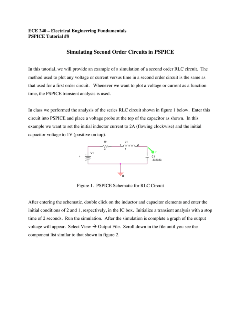
ECE 240 – Electrical Engineering Fundamentals PSPICE Tutorial #8 Simulating Second Order Circuits in PSPICE In this tutorial, we will provide an example of a simulation of a second order RLC circuit. The method used to plot any voltage or current versus time in a second order circuit is the same as that used for a first order circuit. Whenever we want to plot a voltage or current as a function time, the PSPICE transient analysis is used. In class we performed the analysis of the series RLC circuit shown in figure 1 below. Enter this circuit into PSPICE and place a voltage probe at the top of the capacitor as shown. In this example we want to set the initial inductor current to 2A (flowing clockwise) and the initial capacitor voltage to 1V (positive on top). R1 L1 1 4 1 V1 4 2 V C1 .333333 0 Figure 1. PSPICE Schematic for RLC Circuit After entering the schematic, double click on the inductor and capacitor elements and enter the initial conditions of 2 and 1, respectively, in the IC box. Initialize a transient analysis with a stop time of 2 seconds. Run the simulation. After the simulation is complete a graph of the output voltage will appear. Select View à Output File. Scroll down in the file until you see the component list similar to that shown in figure 2. Figure 2. Output File of RLC Circuit We use this listing to determine whether or not the directions (polarity) of the initial conditions are correct. Note that in this case the inductor goes from node N00138 to node N00144. This is the direction that the initial condition current is taken to flow. Since the resistor is also connected to node N00138 we know that this must be the node of the left of the inductor and so the initial condition will flow from left to right as desired. For the capacitor the nodes are 0 (ground) and N00144. The voltage placed in the initial condition box is taken with respect to this node order and hence the positive side of the voltage is at ground. This is opposite the desired direction of the initial condition. To correct this, change the initial condition to -1 . After this correction is made re-simulate the circuit. The output voltage should appear as shown in figure 3. Compare this to the result obtained in class. 4.0V 3.0V 2.0V 1.0V 0s V(C1:2) 0.4s 0.8s 1.2s Time Figure 3. Output of PSPICE Simulation 1.6s 2.0s


