CPC1961
Dual AC Solid State Relays
INTEGRATED CIRCUITS DIVISION
Parameters
Blocking Voltage
AC Operating Voltage
Load Current 1
On State Voltage Drop
1
Ratings
600
260
250
3
Units
VP
Vrms
mArms
Vrms (at IL = 250mArms)
One Pole Operating
Features
•
•
•
•
•
•
•
•
•
•
•
Load Current up to 250 mArms
600VP Blocking Voltage
5mA Sensitivity
Zero-Crossing Detection
DC Control, AC Output
Optically Isolated
TTL and CMOS Compatible
Low EMI and RFI Generation
High Noise Immunity
Machine Insertable, Wave Solderable
Flammability Classification Rating of V-0
Applications
•
•
•
•
•
•
•
•
•
•
Programmable Control
Process Control
Power Control Panels
Remote Switching
Gas Pump Electronics
Contactors
Large Relays
Solenoids
Motors
Heaters
Description
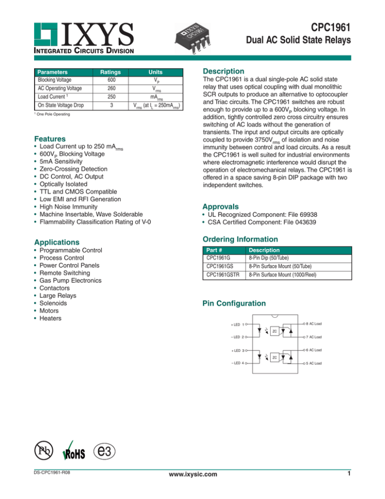
The CPC1961 is a dual single-pole AC solid state
relay that uses optical coupling with dual monolithic
SCR outputs to produce an alternative to optocoupler
and Triac circuits. The CPC1961 switches are robust
enough to provide up to a 600VP blocking voltage. In
addition, tightly controlled zero cross circuitry ensures
switching of AC loads without the generation of
transients. The input and output circuits are optically
coupled to provide 3750Vrms of isolation and noise
immunity between control and load circuits. As a result
the CPC1961 is well suited for industrial environments
where electromagnetic interference would disrupt the
operation of electromechanical relays. The CPC1961 is
offered in a space saving 8-pin DIP package with two
independent switches.
Approvals
• UL Recognized Component: File 69938
• CSA Certified Component: File 043639
Ordering Information
Part #
CPC1961G
CPC1961GS
CPC1961GSTR
Description
8-Pin Dip (50/Tube)
8-Pin Surface Mount (50/Tube)
8-Pin Surface Mount (1000/Reel)
Pin Configuration
8 AC Load
+ LED 1
ZC
7 AC Load
– LED 2
6 AC Load
+ LED 3
ZC
– LED 4
DS-CPC1961-R08
www.ixysic.com
5 AC Load
1
INTEGRATED CIRCUITS DIVISION
CPC1961
Absolute Maximum Ratings @ 25ºC
Parameter
Blocking Voltage
Reverse Input Voltage
Input Control Current
Peak (10ms)
Input Power Dissipation 1
Total Package Dissipation 2
Isolation Voltage, Input to Output
Operational Temperature
Storage Temperature
1
Ratings Units
600
VP
5
VP
50
mA
1
A
150
mW
800
mW
3750
Vrms
-40 to +85
°C
-40 to +125
°C
Absolute Maximum Ratings are stress ratings. Stresses in
excess of these ratings can cause permanent damage to
the device. Functional operation of the device at conditions
beyond those indicated in the operational sections of this
data sheet is not implied.
Derate linearly 1.33 mW / ºC
Derate linearly 6.67 mW / ºC
2
Electrical Characteristics @ 25ºC
Parameters
Output Characteristics
Operating Voltage Range
Load Current 1, Continuous
Non-repetitive Single Cycle Surge Current
Off State Leakage Current
On-State Voltage Drop
Critical Rate of Rise 2
Holding Current
Switching Speeds
Turn-on
Turn-off
Zero-Cross Turn-On Voltage 3
Operating Frequency
Load Power Factor for Guaranteed Turn-On 4
Input Characteristics
Input Control Current to Activate 5
Input Voltage Drop
Input Drop-out Voltage
Reverse Input Current
Common Characteristics
Input to Output Capacitance
Conditions
Symbol
Min
Typ
Max
Units
VL
-
20
-
260
Vrms
VL=120-240Vrms
t < 10ms
VL=600V
IL=250 mArms
IF=5 mA
IL
0.005
500
-
300
250
1
1
3
-
mArms
A
µA
Vrms
V/µs
µA
20
0.25
5
-
0.5
0.5
20
5
500
-
1.2
1.2
-
5
1.4
10
mA
V
V
µA
3
-
pF
IF=5 mA
1st half-cycle
Subsequent half-cycles
-
ITSM
ILEAK
dV/dt
IH
ton
toff
PF
IF=5mA
VR=5V
IF
VF
IR
0.9
0.8
-
-
CI/O
-
cycles
V
V
Hz
-
1
Maximum continuous load current of a single pole or the sum of the load currents with both poles operating simultaneously.
2 Tested in accordance with EIA/NARM standard RS-443.
3 Zero Cross 1st half-cycle @ <100Hz
4 Snubber circuits may be required at low power factors.
5 For high noise environment use at least 10mA LED current.
2
www.ixysic.com
R08
INTEGRATED CIRCUITS DIVISION
CPC1961
PERFORMANCE DATA*
Typical On-State Output
Forward Voltage Distribution
(IF=5mA, IL=250mA, TA=25ºC)
35
Device Count (N)
Device Count (N)
30
25
20
15
10
5
Typical Blocking Voltage Distribution
(IF=0mA, TA=25ºC)
25
25
20
20
Device Count (N)
Typical LED Forward Voltage Drop
(IF=5mA, TA=25ºC)
15
10
5
1.23
2.1
1.24
1.25
1.26
1.27
LED Forward Voltage Drop (V)
10
5
0
0
0
15
2.2
2.3
2.4
On-State Voltage (V)
735
2.5
740
745
750
Blocking Voltage (VP)
755
Typical IF for Switch Operation
(IL=250mA, TA=25ºC)
Device Count (N)
20
15
10
5
0
1.10
LED Forward Voltage vs. Temperature
2.4
IF=50mA
IF=20mA
IF=10mA
1.8
1.3
1.2
IF=5mA
1.4
1.8
1.6
1.4
-20
0
20
40
60
Temperature (ºC)
80
100
1.0
0.6
1.0
0.8
-40
1.2
0.8
1.2
1.1
Typical IF for Switch Dropout
vs. Temperature
(IL=250mA)
1.6
2.0
1.4
1.0
-40
Typical IF for Switch Operation
vs. Temperature
(IL=250mA)
IF Off (mA)
1.5
1.30
2.2
IF On (mA)
LED Forward Voltage (V)
1.6
1.15
1.20
1.25
LED Forward Current (mA)
-20
0
20
40
60
Temperature (ºC)
80
100
0.4
-40
-20
0
20
40
60
Temperature (ºC)
80
100
*The Performance data shown in the graphs above is typical of device performance. For guaranteed parameters not indicated in the written specifications, please
contact our application department.
R08
www.ixysic.com
3
INTEGRATED CIRCUITS DIVISION
CPC1961
PERFORMANCE DATA*
300
2.35
2.30
2.25
2.20
2.15
2.10
20
40
60
Temperature (ºC)
80
100
0
-100
-200
100
140
770
760
750
740
730
720
710
-20
0
20
40
60
Temperature (ºC)
80
100
Maximum Concurrent
Total Load Current vs. Temperature
(IF=5mA)
250
200
150
100
50
0
-3
Leakage Current (nA)
Blocking Voltage (VP)
0
780
-40
200
-300
-20
Typical Blocking Voltage
vs. Temperature
(IF=0mA)
790
300
Load Current (mArms)
Output Current (mA)
On-State Voltage (V)
2.40
2.05
-40
Typical Output Voltage
vs. Output Current
(IF=5mA, TA=25ºC)
-2
-1
0
1
Output Voltage (V)
2
-40
3
Typical Leakage vs. Temperature
Measured Between Pins 5&6 and 7&8
(IF=0mA, VL=600V)
120
100
80
60
40
20
0
-40
-20
0
20
40
60
Temperature (ºC)
80
100
-20
0
20
40
60
Temperature (ºC)
80
100
Maximum Non-Repetitive Surge Current
(TA=25ºC)
Current (A)
2.45
Typical On-State Voltage
vs. Temperature
(IF=5mA, IL=250mA)
1.1
1.0
0.9
0.8
0.7
0.6
0.5
0.4
0.3
0.2
0.1
0.0
0.001
0.01
0.1
1
Time (s)
10
100
*The Performance data shown in the graphs above is typical of device performance. For guaranteed parameters not indicated in the written specifications, please
contact our application department.
4
www.ixysic.com
R08
INTEGRATED CIRCUITS DIVISION
CPC1961
Manufacturing Information
Moisture Sensitivity
All plastic encapsulated semiconductor packages are susceptible to moisture ingression. IXYS Integrated
Circuits Division classified all of its plastic encapsulated devices for moisture sensitivity according to
the latest version of the joint industry standard, IPC/JEDEC J-STD-020, in force at the time of product
evaluation. We test all of our products to the maximum conditions set forth in the standard, and guarantee proper
operation of our devices when handled according to the limitations and information in that standard as well as to any
limitations set forth in the information or standards referenced below.
Failure to adhere to the warnings or limitations as established by the listed specifications could result in reduced
product performance, reduction of operable life, and/or reduction of overall reliability.
This product carries a Moisture Sensitivity Level (MSL) rating as shown below, and should be handled according
to the requirements of the latest version of the joint industry standard IPC/JEDEC J-STD-033.
Device
Moisture Sensitivity Level (MSL) Rating
CPC1961G / CPC1961GS
MSL 1
ESD Sensitivity
This product is ESD Sensitive, and should be handled according to the industry standard JESD-625.
Reflow Profile
This product has a maximum body temperature and time rating as shown below. All other guidelines of J-STD-020
must be observed.
Device
Maximum Temperature x Time
CPC1961G / CPC1961GS
250ºC for 30 seconds
Board Wash
IXYS Integrated Circuits Division recommends the use of no-clean flux formulations. However, board washing to
remove flux residue is acceptable. Since IXYS Integrated Circuits Division employs the use of silicone coating as
an optical waveguide in many of its optically isolated products, the use of a short drying bake could be necessary
if a wash is used after solder reflow processes. Chlorine- or Fluorine-based solvents or fluxes should not be used.
Cleaning methods that employ ultrasonic energy should not be used.
R08
www.ixysic.com
5
INTEGRATED CIRCUITS DIVISION
CPC1961
MECHANICAL DIMENSIONS
CPC1961G
2.540 ± 0.127
(0.100 ± 0.005)
9.652 ± 0.381
(0.380 ± 0.015)
8-0.800 DIA.
(8-0.031 DIA.)
2.540 ± 0.127
(0.100 ± 0.005)
9.144 ± 0.508
(0.360 ± 0.020)
6.350 ± 0.127
(0.250 ± 0.005)
Pin 1
PCB Hole Pattern
7.620 ± 0.254
(0.300 ± 0.010)
6.350 ± 0.127
(0.250 ± 0.005)
0.457 ± 0.076
(0.018 ± 0.003)
3.302 ± 0.051
(0.130 ± 0.002)
7.620 ± 0.127
(0.300 ± 0.005)
7.239 TYP.
(0.285)
4.064 TYP
(0.160)
0.254 ± 0.0127
(0.010 ± 0.0005)
7.620 ± 0.127
(0.300 ± 0.005)
Dimensions
mm
(inches)
0.813 ± 0.102
(0.032 ± 0.004)
CPC1961GS
9.652 ± 0.381
(0.380 ± 0.015)
2.540 ± 0.127
(0.100 ± 0.005)
6.350 ± 0.127
(0.250 ± 0.005)
Pin 1
0.635 ± 0.127
(0.025 ± 0.005)
3.302 ± 0.051
(0.130 ± 0.002)
9.525 ± 0.254
(0.375 ± 0.010)
0.457 ± 0.076
(0.018 ± 0.003)
PCB Land Pattern
2.54
(0.10)
8.90
(0.3503)
1.65
(0.0649)
7.620 ± 0.254
(0.300 ± 0.010)
0.254 ± 0.0127
(0.010 ± 0.0005)
0.65
(0.0255)
4.445 ± 0.127
(0.175 ± 0.005)
Dimensions
mm
(inches)
0.813 ± 0.102
(0.032 ± 0.004)
6
www.ixysic.com
R08
INTEGRATED CIRCUITS DIVISION
CPC1961
CPC1961GSTR Tape & Reel
330.2 DIA.
(13.00 DIA.)
Top Cover
Tape Thickness
0.102 MAX.
(0.004 MAX.)
K0 =4.90
(0.193)
K1 =4.20
(0.165)
Embossed Carrier
Embossment
W=16.00
(0.63)
Bo=10.30
(0.406)
Ao=10.30
(0.406)
P=12.00
(0.472)
User Direction of Feed
Dimensions
mm
(inches)
NOTES:
1. Dimensions carry tolerances of EIA Standard 481-2
2. Tape complies with all “Notes” for constant dimensions listed on page 5 of EIA-481-2
For additional information please visit our website at: www.ixysic.com
IXYS Integrated Circuits Division makes no representations or warranties with respect to the accuracy or completeness of the contents of this publication and reserves the right to make
changes to specifications and product descriptions at any time without notice. Neither circuit patent licenses nor indemnity are expressed or implied. Except as set forth in IXYS Integrated
Circuits Division’s Standard Terms and Conditions of Sale, IXYS Integrated Circuits Division assumes no liability whatsoever, and disclaims any express or implied warranty, relating to
its products including, but not limited to, the implied warranty of merchantability, fitness for a particular purpose, or infringement of any intellectual property right.
The products described in this document are not designed, intended, authorized or warranted for use as components in systems intended for surgical implant into the body, or in other
applications intended to support or sustain life, or where malfunction of IXYS Integrated Circuits Division’s product may result in direct physical harm, injury, or death to a person or severe
property or environmental damage. IXYS Integrated Circuits Division reserves the right to discontinue or make changes to its products at any time without notice.
7
Specification: DS-CPC1961-R08
©Copyright 2013, IXYS Integrated Circuits Division
All rights reserved. Printed in USA.
10/13/2013


