PRODUCT DATASHEET
P50N-UT-A
UV LED
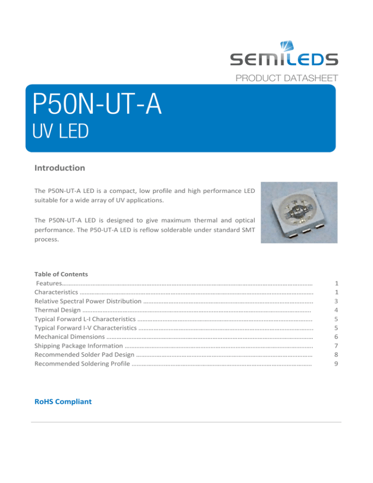
Introduction The P50N‐UT‐A LED is a compact, low profile and high performance LED suitable for a wide array of UV applications. The P50N‐UT‐A LED is designed to give maximum thermal and optical performance. The P50‐UT‐A LED is reflow solderable under standard SMT process. Table of Contents Features………..…………………………………………………………………………………………………………………………
Characteristics ………………………………………………………………………………………………………………………….
Relative Spectral Power Distribution ……………………………………………………………………………………….. Thermal Design ………………………………………………………………………………………………………………………. Typical Forward L‐I Characteristics …………………………………………………………………………………………..
Typical Forward I‐V Characteristics ………………………………………………………………………………………….. Mechanical Dimensions …………………………………………………………………………………………………………… Shipping Package Information ………………………………………………………………………………………………….
Recommended Solder Pad Design …………………………………………………………………………………………… Recommended Soldering Profile ………………..…………………………………………………………………………… RoHS Compliant 1
1
3
4
5
5
6
7
8
9
P50N-UT-A UV LED
Features PRODUCT DATASHEET
Excellent Operating Life SMD Device High Efficacy Instant Light Low Thermal Resistance Fully Dimmable RoHS Compliant Characteristics Absolute Maximum Ratings Rating Parameter UV Maximum DC Forward Current (mA) 180 mA LED Junction Temperature 125℃ LED Operating Temperature ‐40℃~110℃ Storage Temperature ‐40℃~110℃ Soldering Temperature Max. 260℃ / Max. 10sec. (JEDEC 020c) Reverse Voltage Not designed to be driven in reverse bias Preconditioning Acc. to JEDEC Level 3 General Characteristics at 150mA (Tj=25℃) Part number P50N‐UT‐A Color UV Peak Wavelength λp (nm) Min Max 380 420 2θ1/2 Lambertian © 2005‐2013 SemiLEDs. All Right Reserved RoHS Compliant www.semileds.com P50N‐UT‐A Datasheet Rev 2.0 Subject to change without notice
Page 1 P50N-UT-A UV LED
PRODUCT DATASHEET
Part number Color Performance at Test Current (150mA) Group P50N‐UT‐A UV Minimum Radiometric Power (mW) VF Min Max B3 85 2.8 3.8 C1 100 2.8 3.8 C2 120 2.8 3.8 C3 140 2.8 3.8 Remarks: 1. Radiometric power is measured with an accuracy of ±10% 2. The forward voltage is measured with an accuracy of ±0.1V Notes: 1. The peak wavelength is measured with an accuracy of ±1nm 2. Minimum and maximum value refers to the limits and set up of SemiLEDs’ testers. All other measurement data are defined as long‐term production mean values and are only given for reference. 3. A critical component is a component used in a life‐support device or system whose failure can reasonably be expected to cause the failure of that life‐support device or system, or to affect its safety or effectiveness of that device or system. Life support devices or systems are intended (i) to be implanted in the human body, or (ii) to support and/or maintain and sustain human life. If they fail, it is reasonable to assume that the health of the user may be endangered. Components used as a critical component must be approved in writing by SemiLEDs. 4. These devices emit high intensity UV/NUV light. Necessary precautions must be taken during operation. Do not look directly into the light or look through the optical system when in operation. Protective eyewear should be worn at all times during operation. 5. Lens discoloration may occur with prolonged exposure to UV/NUV light. Lens material will need to be tested for UV/NUV light compatibility and durability. Caution: Users are requested to comply with the laws and public regulations concerning safety. © 2005‐2013 SemiLEDs. All Right Reserved RoHS Compliant www.semileds.com P50N‐UT‐A Datasheet Rev 2.0 Subject to change without notice
Page 2 P50N-UT-A UV LED
PRODUCT DATASHEET
Relative Spectral Power Distribution, Tc=25 °C Peak Wavelength (nm)
© 2005‐2013 SemiLEDs. All Right Reserved RoHS Compliant www.semileds.com P50N‐UT‐A Datasheet Rev 2.0 Subject to change without notice
Page 3 P50N-UT-A UV LED
PRODUCT DATASHEET
Thermal Design Thermal design of the end product is important. The thermal resistance between the junction and the solder point (RΘJ‐L) is 10°C/W, and the end product should be designed to minimize the thermal resistance from the solder point to ambient in order to optimize the emitter life and optical characteristics. The maximum operation current is determined by the plot of Allowable Forward Current vs. Ambient Temperature. The junction temperature can be correlated to the thermal resistance between the junction and ambient (Rja) by the following equation. Tj=Ta + Rja*W Tj: LED junction temperature Ta: Ambient temperature Rja: Thermal resistance between the junction and ambient W: Input power ( IF*VF) © 2005‐2013 SemiLEDs. All Right Reserved RoHS Compliant www.semileds.com P50N‐UT‐A Datasheet Rev 2.0 Subject to change without notice
Page 4 P50N-UT-A UV LED
PRODUCT DATASHEET
Typical Forward L‐I Characteristics (Tj=25℃) Typical Forward I‐V Characteristics (Tj=25℃) © 2005‐2013 SemiLEDs. All Right Reserved RoHS Compliant www.semileds.com P50N‐UT‐A Datasheet Rev 2.0 Subject to change without notice
Page 5 P50N-UT-A UV LED
PRODUCT DATASHEET
Mechanical Dimensions ’ Polarity Notes : 1. Drawings are not to scale. 2. All dimensions are in millimeter. 3. General tolerance is ±0.2mm. 4. The polarity of die heat sink at bottom is Anode; please make sure polarity isolation on MCPCB is done correctly. 5. The Cathode is denoted by the bar (minus sign) on plastic body. © 2005‐2013 SemiLEDs. All Right Reserved RoHS Compliant www.semileds.com P50N‐UT‐A Datasheet Rev 2.0 Subject to change without notice
Page 6 P50N-UT-A UV LED
PRODUCT DATASHEET
Shipping Package Information Reel Dimension Carrier Tape Notes : 1. All dimensions are in millimeter 2. Tolerance for fixed dimensions are 0.1mm 3. Packing unit: 1,000pcs/ reel (φ178mm) © 2005‐2013 SemiLEDs. All Right Reserved RoHS Compliant www.semileds.com P50N‐UT‐A Datasheet Rev 2.0 Subject to change without notice
Page 7 P50N-UT-A UV LED
PRODUCT DATASHEET
Recommended Solder Pad Design Notes :
1. Drawing is not to scale
2. All dimensions are in millimeter
© 2005‐2013 SemiLEDs. All Right Reserved RoHS Compliant www.semileds.com P50N‐UT‐A Datasheet Rev 2.0 Subject to change without notice
Page 8 P50N-UT-A UV LED
PRODUCT DATASHEET
Recommended Soldering Profile LEDs can be soldered using the parameter listed below. As a general guideline, the users are suggested to follow the recommended soldering profile provided by the manufacturer of the solder paste. Although the recommended soldering conditions are specified in the list, reflow soldering at the lowest possible temperature is advised for the LEDs. Profile Feature Average Ramp‐up Rate (Tsmax to Tp) Preheat - Temperature Min(Tsmin) - Temperature Max(Tsmax) - Time(tsmin to tsmax) Time maintained above: - Temperature(TL) - Time(tL) Peak/classification Temperature(Tp) Time within 5℃ of actual Peak Temperature(tp) Ramp‐Down Rate Time 25℃ to Peak Temperature Sn‐Pb Eutecitc Assembly
Pb‐Free Assembly 3℃/second max. 3℃/second max. 183℃ 60‐150 seconds 215℃
150℃ 200℃ 60‐180 seconds 217℃ 60‐150 seconds 260℃ 10‐30 seconds 20‐40 seconds 6℃/second max.
6 minutes max. 6℃/second max. 8 minutes max. 100℃ 150℃ 60‐120 seconds © 2005‐2013 SemiLEDs. All Right Reserved RoHS Compliant www.semileds.com P50N‐UT‐A Datasheet Rev 2.0 Subject to change without notice
Page 9 P50N-UT-A UV LED
PRODUCT DATASHEET
About Us SemiLEDs Corporation is a US based manufacturer of ultra‐high brightness LED chips with state of the art fabrication facilities in Hsinchu Science Park, Taiwan. SemiLEDs specializes in the development and manufacturing of vertical LED chips in blue (white), green, and UV using a patented copper alloy base. This unique design allows for higher performance and longer lumen maintenance. In December 2008, The World Economic Forum recognized SemiLEDs innovations with the 2009 Technology Pioneer Award. SemiLEDs is fully ISO 9001:2008 Certified SemiLEDs is a publicly traded company on NASDAQ Global Select Market (stock symbol “LEDS”). For investor information, please contact us at investors@semileds.com. For further company or product information, please visit us at www.semileds.com or please contact sales@ semileds.com. www.semileds.com
ASIA PACIFIC
3F, No. 11, KeJung Rd.
Chu‐Nan Site
Hsinchu Science Park Chu‐Nan 350, Miao‐Li County
Taiwan, ROC Tel: +886‐37‐586788
Fax: +886‐37‐582688
sales@semileds.com
© 2005‐2013 SemiLEDs. All Right Reserved RoHS Compliant www.semileds.com P50N‐UT‐A Datasheet Rev 2.0 Subject to change without notice
Page 10
