9042
12-Bit, 41 MSPS A/D Converter
DESCRIPTION:
• Total dose hardness:
- > 300 krad (Si)
SEL > 120 MeV-cm2/mg
• 41 MSPS minimum sampling rate
• 80 dB Spurious-Free Dynamic Range (SFDR)
• Package:
- 28 pin RAD-PAK® flat pack
• 595 mW power dissipation
• Single 5 volt power supply
• On-chip T/H and reference
• Two’s complement output format
• CMOS compatible output levels
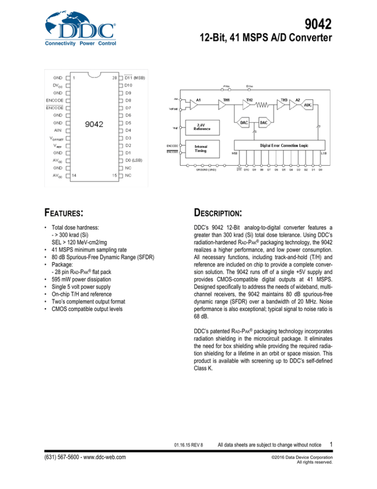
DDC’s 9042 12-Bit analog-to-digital converter features a
greater than 300 krad (Si) total dose tolerance. Using DDC’s
radiation-hardened RAD-PAK® packaging technology, the 9042
realizes a higher performance, and low power consumption.
All necessary functions, including track-and-hold (T/H) and
reference are included on chip to provide a complete conversion solution. The 9042 runs off of a single +5V supply and
provides CMOS-compatible digital outputs at 41 MSPS.
Designed specifically to address the needs of wideband, multichannel receivers, the 9042 maintains 80 dB spurious-free
dynamic range (SFDR) over a bandwidth of 20 MHz. Noise
performance is also exceptional; typical signal to noise ratio is
68 dB.
DDC’s patented RAD-PAK® packaging technology incorporates
radiation shielding in the microcircuit package. It eliminates
the need for box shielding while providing the required radiation shielding for a lifetime in an orbit or space mission. This
product is available with screening up to DDC’s self-defined
Class K.
01.16.15 REV 8
(631) 567-5600 - www.ddc-web.com
All data sheets are subject to change without notice
1
©2016 Data Device Corporation
All rights reserved.
Memory
FEATURES:
9042
12-Bit, 41 MSPS A/D Converter
TABLE 1. 9042 PIN DESCRIPTION
SYMBOL
DESCRIPTION
1
GND
Ground
2
DVCC
5V Power Supply (Digital)
3
GND
Ground
4
ENCODE
Encode Input. Data conversion initiated on rising edge.
5
ENCODE
Complement of ENCODE. Drive differently with ENCODE or bypass
to Ground for single-ended clock mode.
6
GND
Ground
7
GND
Ground
8
AIN
Analog Input.
9
VOFFSET
Voltage Offset Input. Sets mid-point of analog input range. Normally
tied to VREF through 50 Ohm resistor.
10
VREF
Internal Voltage Reference. Nominally 2.4V; normally tied to VOFFSET
through 50 Ohm resistor. Bypass to Ground with 0.01 µF capacitor.
11
GND
Ground
12
AVCC
5V Power Supply (Analog)
13
GND
Ground
14
AVCC
5V Power Supply (Analog)
15
NC
No Connects.
16
NC
No Connects.
17
D0 (LSB)
Digital Output Bit (Least Significant Bit).
18 - 27
D1 - D10
Digital Output Bits.
28
D11 (MSB)1
Memory
PIN
Digital Output Bit (Most Significant Bit).
1. Output coded as twos compliment
01.16.15 REV 8
All data sheets are subject to change without notice
2
©2016 Data Device Corporation
All rights reserved.
9042
12-Bit, 41 MSPS A/D Converter
TABLE 2. 9042 ABSOLUTE MAXIMUM RATINGS1
PARAMETER
SYMBOL
MIN
Analog Supply Voltage
AVCC
Digital Supply Voltage
Analog Input Voltage
TYPICAL
MAX
UNIT
0
7
V
DVCC
0
7
V
AIN
0.5
4.5
V
20
mA
AVCC
V
4
V
40
mA
ELECTRICAL
Analog Input Current
Digital Input Voltage (ENCODE)
0
ENCODE, ENCODE Differential Voltage
Digital Output Current
-40
Package Weight
JC
Thermal Impedance
5.25
Grams
2.39
°C/W
ENVIRONMENTAL
TJ
Operating Temperature Range
TA
Storage Temperature Range
TS
150
°C
-55
125
°C
-65
150
°C
1. Absolute maximum ratings are limiting values to be applied individually, and beyond which the serviceability of the circuit may be impaired. Functional operability is not necessarily
implied. Exposure to absolute maximum rating conditions for an extended period of time may affect device reliability.
TABLE 3. DELTA LIMITS
PARAMETER
VARIATION
I(AVCC)
±10% of specified value in Table 4
I(DVCC)
±10% of specified value in Table 4
ICCTOTAL
±10% of specified value in Table 4
TABLE 4. 9042 DC ELECTRICAL CHARACTERISTICS
(AVCC = DVCC = +5V ±5%; VREF TIED TO VOFFSET THROUGH 50 ; TA = -55°C TO +125°C
PARAMETER
SYMBOL
CONDITION
SUBGROUPS
MIN
Resolution
TYP
MAX
UNIT
10
mV
12
DC ACCURACY
No Missing Codes1
-55 to 125°C
1, 2, 3
Offset Error
-55 to 125°C
1, 2, 3
Offset Tempco
-55 to 125°C
1, 2, 3
Gain Error
-55 to 125°C
1, 2, 3
Gain Tempco
-55 to 125°C
1, 2, 3
25°C
1
REFERENCE OUT
VREF2
01.16.15 REV 8
Guaranteed
-10
±3
25
-6.5
0
ppm/°C
6.5
-50
2.3
2.4
% FS
ppm/°C
2.5
V
All data sheets are subject to change without notice
3
©2016 Data Device Corporation
All rights reserved.
Memory
Maximum Junction Temperature
9042
12-Bit, 41 MSPS A/D Converter
TABLE 4. 9042 DC ELECTRICAL CHARACTERISTICS
(AVCC = DVCC = +5V ±5%; VREF TIED TO VOFFSET THROUGH 50 ; TA = -55°C TO +125°C
PARAMETER
SYMBOL
CONDITION
SUBGROUPS
MIN
TYP
MAX
UNIT
Analog Input (AIN)
Input Voltage Range
1, 2, 3
Input Resistance
-55 to 125°C
2, 3
Input Capacitance
25°C
1
VREF
±0.5
200
250
V
300
7
ENCODE INPUTS1,3
Logic Compatibility4
TTL/
CMOS
Logic “1” Voltage
VIH
-55 to 125°C
1, 2, 3
2.0
5.0
V
Logic “0” Voltage
VIL
-55 to 125°C
1, 2, 3
0
0.8
V
Logic “1” Current (VINH = 5V)
IIH
-55 to 125°C
1, 2, 3
450
625
800
µA
Logic “0” Current (VINL = 0V)
IIL
-55 to 125°C
1, 2, 3
-400
-300
-200
µA
25°C
1
2.5
pF
Memory
Input Capacitance
DIGITAL OUTPUTS
Logic Compatibility
Logic “1” Voltage (IOH = 10 µA)
Logic “0” Voltage (IOL = 10 µA)
CMOS
VOH
VOL
25°C
1
3.5
-55 to 125°C
1, 2, 3
3.5
25°C,125°C
1, 2
-55
3
Output Coding
4.2
--
V
0.80
V
0.90
Twos Compliment
POWER SUPPLY
Analog Supply Voltage
AVCC
-55 to 125°C
1, 2, 3
5.0
Analog Supply Current
I AVCC
-55 to 125°C
1, 2, 3
--
Digital Supply Voltage
DVCC
-55 to 125°C
1, 2, 3
5.0
Digital Supply Current
I DVCC
-55 to 125°C
1, 2, 3
--
20
mA
Supply Current (Total)
ICCTOTAL
-55 to 125°C
1, 2, 3
119
180
mA
-55 to 125°C
1, 2, 3
595
990
mW
25°C
1
±1
20
mV/V
-55 to 125°C
1, 2, 3
Power Dissipation
Power Supply Rejection
PSRR
-20
V
160
mA
V
±5
mV/V
Differential Non-linearity
(ENCODE = 20 MSPS)
DNL
-55 to 125°C
1, 2,3
-1.0
±0.3
1.0
LSB
Integral Non-linearity
(ENCODE = 20 MSPS)
INL
-55 to 125°C
1, 2, 3
-1.5
±0.75
1.5
LSB
1. Guaranteed by design.
2. VREF is normally tied to VOFFSET through 50 ohms. If VREF is used to provide dc offset to other circuits, it should first be buffered
3.
ENCODE driven by single-ended source; ENCODE bypassed to ground through 0.01 µF capacitor.
4.
ENCODE may also be driven differently in conjunction with ENCODE.
01.16.15 REV 8
All data sheets are subject to change without notice
4
©2016 Data Device Corporation
All rights reserved.
9042
12-Bit, 41 MSPS A/D Converter
TABLE 5. 9042 AC ELECTRICAL CHARACTERISTICS1
(AVCC = DVCC = +5V ±5%; ENCODE & ENCODE = 41 MSPS; VREF TIED TO VOFFSET THROUGH 50 ; TA = -55°C TO +125°C)
PARAMETER
Signal to Noise Ratio2, 8
Analog Input @ -1 dBFS
SYMBOL
SUBGROUPS
MIN
TYP
MAX
SNR
1.2 MHz
9.6 MHz
19.5 MHz
SINAD3, 8
Analog Input @ -1 dBFS
CONDITION
dB
25°C
4
--
68
--
-55 to 125°C
5, 6
--
67.5
--
25°C
4
--
67.5
--
-55 to 125°C
5, 6
--
67
--
25°C
4
--
67
--
-55 to 125°C
5, 6
--
66.5
--
SINAD
1.2 MHz
19.5 MHz
dB
25°C
4
--
67.5
--
-55 to 125°C
5, 6
--
67
--
25°C
4
--
67.5
--
-55 to 125°C
5, 6
--
67
--
25°C
4
--
67
--
-55 to 125°C
5, 6
--
66.5
--
Worst Spur4, 8
Analog Input @ -1 dBFS
dBc
1.2 MHz
9.6 MHz
19.5 MHz
Small Signal Spurios Free Dynamic
Range (w/ Dither)5, 8
Analog Input @
1.2 MHz
Memory
9.6 MHz
UNIT
25°C
4
--
80
--
-55 to 125°C
5, 6
--
78
--
25°C
4
--
80
--
-55 to 125°C
5, 6
--
78
--
25°C
4
--
80
--
-55 to 125°C
5, 6
--
78
--
SFDR
dBFS
-55 to 125°C
4, 5, 6
--
90
--
9.6 MHz
--
90
--
19.5 MHz
--
90
--
Two-Tone IMD Rejection6
F1, F2 @ -7 dBFS
-55 to 125°C
4, 5, 6
--
80
--
dBc
Two-Tone SFDR (w/Dither)7
-55 to 125°C
4, 5, 6
--
90
--
dBFS
Thermal Noise
25°C
9
--
0.33
--
LSB rms
Analog Input bandwidth8
25°C
9
100
MHz
Transient Response8
25°C
9
10
ns
Overvoltage Recovery Time8
25°C
9
25
ns
01.16.15 REV 8
All data sheets are subject to change without notice
5
©2016 Data Device Corporation
All rights reserved.
9042
12-Bit, 41 MSPS A/D Converter
TABLE 5. 9042 AC ELECTRICAL CHARACTERISTICS1
(AVCC = DVCC = +5V ±5%; ENCODE & ENCODE = 41 MSPS; VREF TIED TO VOFFSET THROUGH 50 ; TA = -55°C TO +125°C)
PARAMETER
SYMBOL
CONDITION
SUBGROUPS
MIN
-55 to 125°C
9, 10, 11
41
tA
25°C
9
-250
ps
Jitter
25°C
9
0.7
ps rms
ENCODE Pulse Width High
25°C
9
10
ns
ENCODE Pulse Width Low
25°C
9
10
ns
-55 to 125°C
9, 10, 11
5
Maximum Conversion Rate
Aperature Delay
Aperature Uncertainty
Output Delay
1.
2.
3.
4.
5.
6.
7.
8.
tOD
TYP
MAX
UNIT
MSPS
9
14
ns
All AC specifications tested by driving ENCODE and ENCODE differentially.
Analog input signal power at -1 dBFS; signal-to-noise ratio (SNR) is the ratio of signal level to total noise (first five harmonics removed).
Analog input signal power at -1 dBFS; signal-to-noise and distorsion (SINAD) is the ratio of signal level to total noise + harmonics.
Analog input signal power at -1 dBFS; worst spur is the ratio of signal level to worst spur, usually limited by harmonics.
Analog input signal power swept from -20 dBFS to -95 dBFS; dither power = -32.5 dBm; dither circuit used on input signal SFDR is ratio of converter full scale to worst spur.
Tones at -7dBFS (F1 = 15.3 MHz, F2 = 19.5 MHz); two tone intermodualtion distortion (IMD) rejection is ratio or either tone to worst third order intermod product.
Both input tones swept from -20 to -95 dBFS; dither power = -32.5 dBm; dither circuit used on input signal two-tone spurious-free dynamic range (SFDR) is the ratio of converter full
scale to worst spur.
Guaranteed by design.
Memory
FIGURE 1. TIMING DIAGRAM
01.16.15 REV 8
All data sheets are subject to change without notice
6
©2016 Data Device Corporation
All rights reserved.
9042
12-Bit, 41 MSPS A/D Converter
FIGURE 2. ANALOG INPUT STAGE EQUIVALENT CIRCUIT
Memory
FIGURE 3. ENCODE INPUTS EQUIVALENT CIRCUIT
01.16.15 REV 8
All data sheets are subject to change without notice
7
©2016 Data Device Corporation
All rights reserved.
9042
12-Bit, 41 MSPS A/D Converter
FIGURE 4. COMPENSATION PIN, C1 EQUIVALENT CIRCUIT
Memory
01.16.15 REV 8
All data sheets are subject to change without notice
8
©2016 Data Device Corporation
All rights reserved.
9042
12-Bit, 41 MSPS A/D Converter
FIGURE 5. DIGITAL OUTPUT STAGE EQUIVALENT CIRCUIT
Memory
FIGURE 6. 2.4 V REFERENCE EQUIVALENT CIRCUIT
01.16.15 REV 8
All data sheets are subject to change without notice
9
©2016 Data Device Corporation
All rights reserved.
9042
12-Bit, 41 MSPS A/D Converter
FIGURE 7. SINGLE TONE AT 1.2 MHZ
Memory
FIGURE 8. SINGLE TONE AT 9.6 MHZ
01.16.15 REV 8
All data sheets are subject to change without notice
10
©2016 Data Device Corporation
All rights reserved.
9042
12-Bit, 41 MSPS A/D Converter
FIGURE 9. SINGLE TONE AT 19.5 MHZ
Memory
FIGURE 10. HARMONICS VS. AIN
01.16.15 REV 8
All data sheets are subject to change without notice
11
©2016 Data Device Corporation
All rights reserved.
9042
12-Bit, 41 MSPS A/D Converter
FIGURE 11. NOISE VS. AIN
Memory
FIGURE 12. HARMONICS VS. AIN
01.16.15 REV 8
All data sheets are subject to change without notice
12
©2016 Data Device Corporation
All rights reserved.
9042
12-Bit, 41 MSPS A/D Converter
FIGURE 13. TWO TONES AT 15.3 MHZ AND 19.5 MHZ
Memory
FIGURE 14. SINGLE TONE SFDR
01.16.15 REV 8
All data sheets are subject to change without notice
13
©2016 Data Device Corporation
All rights reserved.
9042
12-Bit, 41 MSPS A/D Converter
FIGURE 15. TWO TONES SFDR
Memory
FIGURE 16. SNR WORST HARMONIC VS. ENCODE
01.16.15 REV 8
All data sheets are subject to change without notice
14
©2016 Data Device Corporation
All rights reserved.
9042
12-Bit, 41 MSPS A/D Converter
FIGURE 17. SNR WORST CASE SPURIOUS VS. DUTY CYCLE
Memory
FIGURE 18. NPR OUTPUT SPECTRUM
01.16.15 REV 8
All data sheets are subject to change without notice
15
©2016 Data Device Corporation
All rights reserved.
9042
12-Bit, 41 MSPS A/D Converter
THEORY OF OPERATION
The 9042 analog-to-digital converter (ADC) employs a twostage subrange architecture. This design approach ensures
12-bit accuracy, without the need for laser trim, at low power. As shown in the functional block diagram, the 1 V p-p
SingleEnded analog input, centered at 2.4 V, drives a single-in to differential-out amplifier, A1. The output of A1 drives
the first track-and-hold, TH1. The high state of the ENCODE pulse places TH1 in hold mode. The held value of TH1 is
applied to the input of the 6-bit coarse ADC. The digital output of the coarse ADC drives a 6-bit DAC; the DAC is 12
bits accurate. The output of the 6-bit DAC is subtracted from the delayed analog signal at the input to TH3 to generate
a residue signal. TH2 is used as an analog pipeline to null out the digital delay of the coarse ADC. The residue signal
is passed to TH3 on a subsequent clock cycle where the signal is amplified by the residue amplifier, A2, and converted
to a digital word by the 7-bit residue ADC. One bit of overlap is used to accommodate any linearity errors in the coarse
ADC.
The 6-bit coarse ADC word and 7-bit residue word are added together and corrected in the digital error correction logic
to generate the output word. The result is a 12-bit parallel digital word which is CMOS-compatible, coded as twos complement.
APPLYING THE 9042
The 9042 is designed to interface with TTL and CMOS logic families. The source used to drive the ENCODE pin(s)
must be clean and free from jitter. Sources with excessive jitter will limit SNR (ref. Equation 1 under “Noise Floor and
SNR”).
Figure 19. Single-Ended TTL/CMOS Encode
01.16.15 REV 8
All data sheets are subject to change without notice
16
©2016 Data Device Corporation
All rights reserved.
Memory
Encoding the 9042
9042
12-Bit, 41 MSPS A/D Converter
The 9042 encode inputs are connected to a differential input stage (See Figure 3). With no input connected to either
the ENCODE or input, the voltage dividers bias the inputs to 1.6 volts. For TTL or CMOS usage, the encode source
should be connected to ENCODE. ENCODE should be decoupled using a low inductance or microwave chip capacitor
to ground. Devices such as AVX 05085C103MA15, a 0.01 mF capacitor, work well.
If a logic threshold other than the nominal 1.6 V is required, the following equations show how to use an external resistor, RX, to raise or lower the trip point (See Figure 3; R1 = 17k, R2 = 8k).
to lower logic threshold.
Figure 20. Lower Logic Threshold for Encode
Memory
to raise logic threshold.
01.16.15 REV 8
All data sheets are subject to change without notice
17
©2016 Data Device Corporation
All rights reserved.
9042
12-Bit, 41 MSPS A/D Converter
Figure 21. Raise Logic Threshold for Encode
Memory
While the single-ended encode will work well for many applications, driving the encode differentially will provide
increased performance. Depending on circuit layout and system noise, a 1 dB to 3 dB improvement in SNR can be
realized. It is not recommended that differential TTL logic be used however, because most TTL families that support
complementary outputs are not delay or slew rate matched. Instead, it is recommended that the encode signal be accoupled into the ENCODE and ENCODE pins.
The simplest option is shown below. The low jitter TTL signal is coupled with a limiting resistor, typically 100 ohms, to
the primary side of an RF transformer (these transformers are inexpensive and readily available; part# in Figure 22 is
from Mini-Circuits). The secondary side is connected to the ENCODE and ENCODE pins of the converter. Since both
encode inputs are self biased, no additional components are required.
Figure 22. TTL Source – Differential Encode
01.16.15 REV 8
All data sheets are subject to change without notice
18
©2016 Data Device Corporation
All rights reserved.
9042
12-Bit, 41 MSPS A/D Converter
Figure 23. Sine Source – Differential Encode
If a low jitter ECL clock is available, another option is to accouple a differential ECL signal to the encode input pins as
shown below. The capacitors shown here should be chip capacitors but do not need to be of the low inductance variety.
Figure 24. Differential ECL for Encode
01.16.15 REV 8
All data sheets are subject to change without notice
19
©2016 Data Device Corporation
All rights reserved.
Memory
If no TTL source is available, a clean sine wave may be substituted. In the case of the sine source, the matching network is shown below. Since the matching transformer specified is a 1:1 impedance ratio, R, the load resistor should be
selected to match the source impedance. The input impedance of the 9042 is negligible in most cases.
9042
12-Bit, 41 MSPS A/D Converter
As a final alternative, the ECL gate may be replaced by an ECL comparator. The input to the comparator could then be
a logic signal or a sine signal.
Figure 25. ECL Comparator for Encode
Memory
Care should be taken not to overdrive the encode input pin when ac coupled. Although the input circuitry is electrically
protected from over or under voltage conditions, improper circuit operations may result from overdriving the encode
input pins.
Driving the Analog Input
Because the 9042 operates off of a single +5 V supply, the analog input range is offset from ground by 2.4 volts. The
analog input, AIN, is an operational amplifier configured in an inverting mode (ref. Equivalent Circuits: Analog Input
Stage). VOFFSET is the noninverting input which is normally tied through a 50 ohm resistor to VREF (ref. Equivalent
Circuits: 2.4 V Reference). Since the operational amplifier forces its inputs to the same voltage, the inverting input is
also at 2.4 volts. Therefore, the analog input has a Thevenin equivalent of 250 ohms in series with a 2.4 volt source. It
is strongly recommended that the 9042’s internal voltage reference be used for the amplifier offset; this reference is
designed to track internal circuit shifts over temperature.
01.16.15 REV 8
All data sheets are subject to change without notice
20
©2016 Data Device Corporation
All rights reserved.
9042
12-Bit, 41 MSPS A/D Converter
Figure 26. Analog Input Offset by +2.4 V Reference
Memory
Although the 9042 may be used in many applications, it was specifically designed for communications systems which
must digitize wide signal bandwidths. As such, the analog input was designed to be ac-coupled. Since most communications products do not down-convert to dc, this should not pose a problem. One example of a typical analog input circuit is shown below. In this application, the analog input is coupled with a high quality chip capacitor, the value of which
can be chosen to provide a low frequency cutoff that is consistent with the signal being sampled; in most cases, a 0.1
mF chip capacitor will work well.
Figure 27. AC-Coupled Analog Input Signal
01.16.15 REV 8
All data sheets are subject to change without notice
21
©2016 Data Device Corporation
All rights reserved.
9042
12-Bit, 41 MSPS A/D Converter
Another option for ac-coupling is a transformer. The impedance ratio and frequency characteristics of the transformer
are determined by examining the characteristics of the input signal source (transformer primary connection), and the
9042 input characteristics (transformer secondary connection). “RT” should be chosen to satisfy termination requirements of thesource, given the transformer turns ratio. A blocking capacitor is required to prevent 9042 dc bias currents
from flowing through the transformer.
Figure 28. Transformer-Coupled Analog Input Signal
where Z is desired impedance.
9042
A dc-coupled input configuration (shown below) is limited by the drive amplifier performance. The 9042’s on-chip reference is buffered using the OP279 dual, rail-to-rail operational amplifier. The resulting voltage is combined with the
analog source using an AD9631. Pending improvements in drive amplifiers, this dc-coupled approach is limited to ~75
dB–80 dB of dynamic performance depending on which drive amplifier is used. The AD9631 and OP279 run off ±5 V.
Figure 29. DC-Coupled Analog Input Circuit
01.16.15 REV 8
All data sheets are subject to change without notice
22
©2016 Data Device Corporation
All rights reserved.
Memory
When calculating the proper termination resistor, note that the external load resistor is in parallel with the 9042 analog
input resistance, 250 ohms. The external resistor value can be calculated from the following equation:
12-Bit, 41 MSPS A/D Converter
9042
Power Supplies
Output Loading
Care must be taken when designing the data receivers for the AD9042. It is recommended that the digital outputs
drive a series resistor of 499 ohms followed by a CMOS gate like the 74AC574. To minimize capacitive loading, there
should only be one gate on each output pin. The digital outputs of the 9042 have a unique constant slew rate output
stage. The output slew rate is about 1 V/ns independent of output loading. A typical CMOS gate combined with PCB
trace and through hole will have a load of approximately 10 pF. Therefore as each bit switches, 10 mA
of dynamic current per bit will flow in or out of the device. A full- scale transition can cause up to 120 mA (12bits ´ 10
mA/bit) of current to flow through the digital output stage. The series resistor will minimize the output currents that can
flow in the output stage. These switching currents are confined between ground and the DVCC pin. Standard TTL gates
should be avoided since they can appreciably add to the dynamic switching currents of the 9042.
01.16.15 REV 8
All data sheets are subject to change without notice
23
©2016 Data Device Corporation
All rights reserved.
Memory
Care should be taken when selecting a power source. Linear supplies are strongly recommended as switching supplies tend to have radiated components that may be “received” by the 9042. Each of the power supply pins should be
decoupled as closely to the package as possible using 0.1 mF chip capacitors. The 9042 has separate digital and analog +5 V pins. The analog supplies and the denoted AVCC digital supply pins are denoted DVCC. Although analog and
digital supplies may be tied together, best performance is achieved when the supplies are separate. This is because
the fast digital output swings can couple switching noise back into the analog supplies. Note that AVCC must be held
within 5% of 5 volts, however the DVCC supply may be varied according to output digital logic family (i.e., DVCC should
be connected to the supply for the digital circuitry).
9042
12-Bit, 41 MSPS A/D Converter
Memory
28-PIN RAD-PAK® FLAT PACKAGE
DIMENSION
SYMBOL
MIN
NOM
MAX
A
0.129
0.142
0.155
b
0.015
0.017
0.022
c
0.004
0.005
0.009
D
--
0.820
0.828
E
0.474
0.480
0.486
E1
--
--
0.506
E2
0.255
0.260
--
E3
0.000
0.110
--
e
0.050 BSC
L
0.375
0.385
0.395
Q
0.021
0.025
0.029
S1
0.000
0.077
--
N
28
Note: All dimensions in inches
01.16.15 REV 8
All data sheets are subject to change without notice
24
©2016 Data Device Corporation
All rights reserved.
12-Bit, 41 MSPS A/D Converter
9042
Important Notice:
These data sheets are created using the chip manufacturer’s published specifications. DDC verifies functionality by
testing key parameters either by 100% testing, sample testing or characterization.
The specifications presented within these data sheets represent the latest and most accurate information available to
date. However, these specifications are subject to change without notice and DDC assumes no responsibility for the
use of this information.
DDC’s products are not authorized for use as critical components in life support devices or systems without express
written approval from DDC.
Any claim against DDC must be made within 90 days from the date of shipment from DDC. DDC’s liability shall be limited to replacement of defective parts.
Memory
01.16.15 REV 8
All data sheets are subject to change without notice
25
©2016 Data Device Corporation
All rights reserved.
9042
12-Bit, 41 MSPS A/D Converter
Product Ordering Options
Model Number
9042
RP
F
X
Option Details
Feature
Screening Flow
MCM1
K= DDC Self-Defined Class K
H= DDC Self-Defined Class H
I = Industrial (testing @ -55°C,
+25°C, +125°C)
E = Engineering (testing @ +25°C)
F = Flat Pack
Radiation Feature
RP = RAD-PAK® package
Base Product
Nomenclature
12-Bit, 41 MSPS A/D Converter
Memory
Package
1) Products are manufactured and screened to DDC’s self-defined Class H and Class K flows.
01.16.15 REV 8
All data sheets are subject to change without notice
26
©2016 Data Device Corporation
All rights reserved.
