The Accelerating Demand for EOS TVS … Over the past five years
advertisement

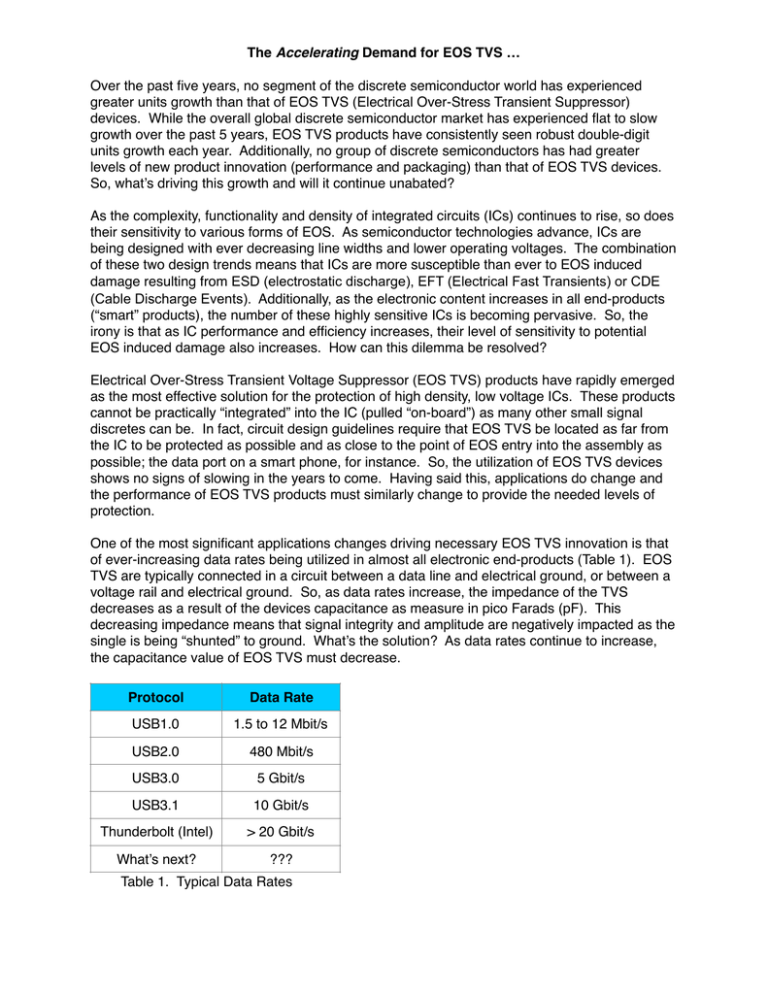
The Accelerating Demand for EOS TVS … Over the past five years, no segment of the discrete semiconductor world has experienced greater units growth than that of EOS TVS (Electrical Over-Stress Transient Suppressor) devices. While the overall global discrete semiconductor market has experienced flat to slow growth over the past 5 years, EOS TVS products have consistently seen robust double-digit units growth each year. Additionally, no group of discrete semiconductors has had greater levels of new product innovation (performance and packaging) than that of EOS TVS devices. So, what’s driving this growth and will it continue unabated? As the complexity, functionality and density of integrated circuits (ICs) continues to rise, so does their sensitivity to various forms of EOS. As semiconductor technologies advance, ICs are being designed with ever decreasing line widths and lower operating voltages. The combination of these two design trends means that ICs are more susceptible than ever to EOS induced damage resulting from ESD (electrostatic discharge), EFT (Electrical Fast Transients) or CDE (Cable Discharge Events). Additionally, as the electronic content increases in all end-products (“smart” products), the number of these highly sensitive ICs is becoming pervasive. So, the irony is that as IC performance and efficiency increases, their level of sensitivity to potential EOS induced damage also increases. How can this dilemma be resolved? Electrical Over-Stress Transient Voltage Suppressor (EOS TVS) products have rapidly emerged as the most effective solution for the protection of high density, low voltage ICs. These products cannot be practically “integrated” into the IC (pulled “on-board”) as many other small signal discretes can be. In fact, circuit design guidelines require that EOS TVS be located as far from the IC to be protected as possible and as close to the point of EOS entry into the assembly as possible; the data port on a smart phone, for instance. So, the utilization of EOS TVS devices shows no signs of slowing in the years to come. Having said this, applications do change and the performance of EOS TVS products must similarly change to provide the needed levels of protection. One of the most significant applications changes driving necessary EOS TVS innovation is that of ever-increasing data rates being utilized in almost all electronic end-products (Table 1). EOS TVS are typically connected in a circuit between a data line and electrical ground, or between a voltage rail and electrical ground. So, as data rates increase, the impedance of the TVS decreases as a result of the devices capacitance as measure in pico Farads (pF). This decreasing impedance means that signal integrity and amplitude are negatively impacted as the single is being “shunted” to ground. What’s the solution? As data rates continue to increase, the capacitance value of EOS TVS must decrease. Protocol Data Rate USB1.0 1.5 to 12 Mbit/s USB2.0 480 Mbit/s USB3.0 5 Gbit/s USB3.1 10 Gbit/s Thunderbolt (Intel) > 20 Gbit/s What’s next? ??? Table 1. Typical Data Rates The technology roadmaps of EOS TVS are the result of some specific end-market demands relative to electrical and mechanical performance. As mentioned, capacitance is quickly becoming the most important device parameter to design engineers. What was known as a “low capacitance” device several years ago, is now seen as a high capacitance device not suitable for many of the newer high speed data protocols. It is widely accepted that USB3.0 and faster data rates must have EOS TVS devices with capacitance values below 0.6pF; anything higher will result in unacceptable signal attenuation. In addition, devices must have a very tight “clamping ratio.” The clamping ratio is a measure of how closely the EOS will clamp (maximum allowable voltage under surge) relative to the working reverse voltage of the device (normal circuit operating voltage). In an ideal world, the clamping voltage rating, VC, and the reverse working voltage rating, VRWM, would be equal. In reality, however, VC is higher than VRWM. In some technology types, VC / VRWM is much greater than one (4.0 or greater); design engineers seek devices with the lowest possible VC / VRWM . Regarding mechanical considerations (packaging), lower profile (thin) end-products are driving the need for lower profile semiconductor packages. Certain EOS TVS technology types do not lend themselves well to low profile packaging by nature of their “inner workings.” Silicon based devices, however, with their thin silicon die configured parallel to the circuit board, make possible very thin, low profile packages. Presently, device types with package profiles below 0.4mm are available from some manufacturers. One final word regarding device performance relative to standby power, or idle current. It is very possible that an EOS TVS might, during its lifetime, be called into action (having to clamp an EOS transient) only once or twice. So, what is it doing the other 99.9% of the time? Hopefully nothing. In the ideal world, when the EOS TVS is “idle” it is completely invisible to the circuit and consuming no power. In reality, however, EOS TVS devices while sitting “idle” will conduct a very small leakage current. This leakage current translates into energy inefficiency. Hence, design engineers seek EOS TVS technologies that afford the lowest levels of standby power consumption. EOS TVS come in many different technologies. Table 2 demonstrates the real world of tradeoffs and compromise that engineers are confronted with each and every day. The variety of technologies, package types and costs give engineers plenty to consider. Unfortunately, no one device does it all, but there are device types that afford the fewest amount of trade-offs while at the same time satisfying critical design requirements. SMC Diode Solutions believes they have achieved the best of all worlds with their eGuard™ series of silicon based EOS suppressors. The eGuard™ series targets the most critical requirements of the design community; namely, ultralow capacitance, tight clamping ratio, low idle current and low profile packaging. Technology Capacitance Clamping Ratio Max Energy Standby Power Low Profile Varistor Poor Poor Very Good Good Poor Ceramic Very Good Good Good Good Good Silicon Very Good Very Good Good Very Good Very Good Table 2. Prevalent EOS Technology Types The trends are clear and irreversible. ICs are becoming higher density, lower voltage and, hence, more susceptible to potential EOS damage. Additionally, data rates continue to increase and electronic content growth in all end-use products is seemingly exponential. The task for design engineers is formidable when it comes to EOS selection. The “best device” is the one that requires the fewest trade-offs, provides the best overall performance and satisfies challenging mechanical concerns for space constrained applications. SMC Diode Solutions has put together a very broad EOS portfolio that features ultra low capacitance devices, such as the new eGuard™ series, and a vast variety or single line and multi-line arrays, such as the SMDA series. Each series has benefits and attributes that make it ideal for a particular set of applications. SMC’s knowledgeable sales and applications team will assist in device selection to ensure the optimal solution is achieved each and every time.


