Design of Broadband mm-Wave Low Noise Amplifiers in CMOS
advertisement

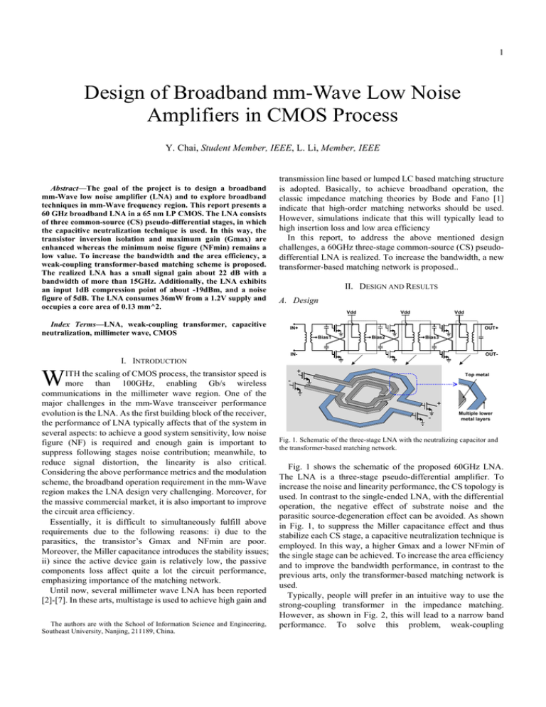
1 Design of Broadband mm-Wave Low Noise Amplifiers in CMOS Process Y. Chai, Student Member, IEEE, L. Li, Member, IEEE Abstract—The goal of the project is to design a broadband mm-Wave low noise amplifier (LNA) and to explore broadband techniques in mm-Wave frequency region. This report presents a 60 GHz broadband LNA in a 65 nm LP CMOS. The LNA consists of three common-source (CS) pseudo-differential stages, in which the capacitive neutralization technique is used. In this way, the transistor inversion isolation and maximum gain (Gmax) are enhanced whereas the minimum noise figure (NFmin) remains a low value. To increase the bandwidth and the area efficiency, a weak-coupling transformer-based matching scheme is proposed. The realized LNA has a small signal gain about 22 dB with a bandwidth of more than 15GHz. Additionally, the LNA exhibits an input 1dB compression point of about -19dBm, and a noise figure of 5dB. The LNA consumes 36mW from a 1.2V supply and occupies a core area of 0.13 mm^2. Index Terms—LNA, weak-coupling transformer, capacitive neutralization, millimeter wave, CMOS W I. INTRODUCTION ITH the scaling of CMOS process, the transistor speed is more than 100GHz, enabling Gb/s wireless communications in the millimeter wave region. One of the major challenges in the mm-Wave transceiver performance evolution is the LNA. As the first building block of the receiver, the performance of LNA typically affects that of the system in several aspects: to achieve a good system sensitivity, low noise figure (NF) is required and enough gain is important to suppress following stages noise contribution; meanwhile, to reduce signal distortion, the linearity is also critical. Considering the above performance metrics and the modulation scheme, the broadband operation requirement in the mm-Wave region makes the LNA design very challenging. Moreover, for the massive commercial market, it is also important to improve the circuit area efficiency. Essentially, it is difficult to simultaneously fulfill above requirements due to the following reasons: i) due to the parasitics, the transistor’s Gmax and NFmin are poor. Moreover, the Miller capacitance introduces the stability issues; ii) since the active device gain is relatively low, the passive components loss affect quite a lot the circuit performance, emphasizing importance of the matching network. Until now, several millimeter wave LNA has been reported [2]-[7]. In these arts, multistage is used to achieve high gain and The authors are with the School of Information Science and Engineering, Southeast University, Nanjing, 211189, China. transmission line based or lumped LC based matching structure is adopted. Basically, to achieve broadband operation, the classic impedance matching theories by Bode and Fano [1] indicate that high-order matching networks should be used. However, simulations indicate that this will typically lead to high insertion loss and low area efficiency In this report, to address the above mentioned design challenges, a 60GHz three-stage common-source (CS) pseudodifferential LNA is realized. To increase the bandwidth, a new transformer-based matching network is proposed.. II. DESIGN AND RESULTS A. Design Vdd Vdd Vdd OUT+ IN+ Bias1 Bias2 Bias3 OUT- IN- + Top metal - + - Multiple lower metal layers Fig. 1. Schematic of the three-stage LNA with the neutralizing capacitor and the transformer-based matching network. Fig. 1 shows the schematic of the proposed 60GHz LNA. The LNA is a three-stage pseudo-differential amplifier. To increase the noise and linearity performance, the CS topology is used. In contrast to the single-ended LNA, with the differential operation, the negative effect of substrate noise and the parasitic source-degeneration effect can be avoided. As shown in Fig. 1, to suppress the Miller capacitance effect and thus stabilize each CS stage, a capacitive neutralization technique is employed. In this way, a higher Gmax and a lower NFmin of the single stage can be achieved. To increase the area efficiency and to improve the bandwidth performance, in contrast to the previous arts, only the transformer-based matching network is used. Typically, people will prefer in an intuitive way to use the strong-coupling transformer in the impedance matching. However, as shown in Fig. 2, this will lead to a narrow band performance. To solve this problem, weak-coupling 2 transformers are used in the last two stages of the LNA, achieving the broadband impedance matching. As shown in Fig. 1, in the second winding, lower metals are used, realizing the weak-coupling transformer (the coupling coefficient k is about 0.4). As a result, the bandwidth is increased substantially. According to Fig. 2, compared to the strong-coupling matching scheme, with the weak-coupling transformer matching network, the bandwidth is improved by 150%. It should be noted that the weak-coupling transformer insertion loss can be as low as 1dB in the targeting band. In other words, it will not deteriorate the total gain performance. ΓOUT1 Γ S1 Fig. 3. Chip micrograph of the proposed LNA. 30 ΓOUT1 Magnitude (dB) 20 ΓOUT1 ΓS1 ΓS1 10 0 -10 -20 40 Available gain (dB) 30 S11 S21 S22 45 50 55 Frequency (GHz) 60 65 Fig. 4. Measured S-parameters of the realized LNA. 25 IV. NEXT CAREER PLANS 20 15 10 strong coupling weak coupling 5 0 50 55 60 65 Frequency (GHz) 70 75 I am going to pursue my PhD degree in Southeast University, China. I really appreciate the help from the MTT-S Scholarship program, which encourages me to continue my research on the mm-Wave circuit design. Fig. 2. Comparison between the matching strategies of a strong- coupling transformer and a weak-coupling transformer. REFERENCES [1] B. Results The LNA is realized in a standard 65 nm LP CMOS process. The chip micrograph is shown in Fig. 3. Including all the testing pads, the LNA occupies 880 μm × 600 μm area, while the core area is only 880 μm × 150 μm. The measured S-parameters are shown in Fig. 4. The circuit achieves a small-signal power gain of 22 dB. Due to the equipment frequency limit, the circuit can only be measured up to 67GHz, ending up >15 GHz bandwidth. The P1dB of the LNA is about -19 dBm. Since we are lack of the noise measurement equipment, here we give the simulated noise performance. The minimum NF is about 4.2 dB. III. CONCLUSION With the help of the capacitive neutralization and the weak-coupling transformer-based matching network, the presented LNA achieves more than 15 GHz bandwidth without deteriorating the gain performance. Caused by the beauty of the transformer matching, the area efficiency is improved. The total chip core area is only about 0.13 mm2. [2] [3] [4] [5] [6] [7] [8] R. M. Fano, “Theoretical limitations on the broadband matching of arbitrary impedances,” J. Franklin Institute, vol. 249, pp. 57-83 and 139-155, Jan. and Feb. 1950. N. Li, K. Bunsen, N. Takayama, Q. Bu, T. Suzuki, M. Sato, T. Hi-rose, K. Okada, and A. Matsuzawa, “A 24 dB gain 51–68 GHz CMOS low noise amplifier using asymmetric-layout transistors,” in Proc. ES-SCIRC, Sept. 2010, pp. 342–345 T. Yao, M. Q. Gordon, K. K. W. Tang, K. H. K. Yau, M. Yang, P. Schvan, and S. P. Voinigescu, “Algorithmic Design of CMOS LNAs and PAs for 60-GHz Radio,” IEEE J. Solid-State Circuits, vol. 42, no. 5, May. 2007. S. Pellerano, Y. Palaskas, K. Soumyanath, “A 64 GHz LNA With 15.5 dB Gain and 6.5 dB NF in 90 nm CMOS,” IEEE J. Solid-State Circuits, vol.43, no.7, pp.1542-1552, July 2008. Y. Natsukari, M. Fujishima, “36mW 63GHz CMOS differential low-noise amplifier with 14GHz bandwidth,” IEEE VLSI Circuit Symp., pp.252-253, Jun. 2009 Q. Bu, N. Li, K. Okada, and A. Matsuzawa, “A Wideband LNA with an Excellent Gain Flatness for 60 GHz 16QAM Modulation in 65 nm CMOS,” in Proc. APMC 2011, pp. 359 – 362. Y. Hsieh, J. Kuo, H. Wang, and L. Lu, “A 60 GHz Broadband Low-Noise Amplifier With Variable-Gain Control in 65 nm CMOS”, IEEE Microwave and Wireless Component Letters, vol. 21, no. 11, Nov. 2011 T., Wang, T. Mitomo, N. Ono, and O. Watanabe, “A 55-67GHz Power Amplifier with 13.6% PAE in 65 nm standard CMOS,” IEEE RFIC Symp. 2011.


