UNISONIC TECHNOLOGIES CO., LTD TA7368P
advertisement

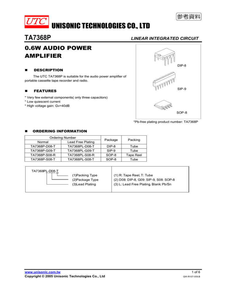
参考資料 UNISONIC TECHNOLOGIES CO., LTD TA7368P LINEAR INTEGRATED CIRCUIT 0.6W AUDIO POWER AMPLIFIER DIP-8 DESCRIPTION The UTC TA7368P is suitable for the audio power amplifier of portable cassette tape recorder and radio. SIP-9 FEATURES * Very few external components( only three capacitors) * Low quiescent current * High voltage gain: Gv=40dB SOP-8 *Pb-free plating product number: TA7368P ORDERING INFORMATION Ordering Number Normal Lead Free Plating TA7368P-D08-T TA7368PL-D08-T TA7368P-G09-T TA7368PL-G09-T TA7368P-S08-R TA7368PL-S08-R TA7368P-S08-T TA7368PL-S08-T Package Packing DIP-8 SIP-9 SOP-8 SOP-8 Tube Tube Tape Reel Tube TA7368PL-D08-T (1)Packing Type (2)Package Type (3)Lead Plating www.unisonic.com.tw Copyright © 2005 Unisonic Technologies Co., Ltd (1) R: Tape Reel, T: Tube (2) D08: DIP-8, G09: SIP-9, S08: SOP-8 (3) L: Lead Free Plating, Blank: Pb/Sn 1 of 6 QW-R107-009,B 参考資料 TA7368P LINEAR INTEGRATED CIRCUIT PIN DESCRIPTION SOP-8/DIP-8 V IN 1 8 Vcc RIPPLE 2 7 POUT NF 3 6 PWR-GND PHASE 4 5 PRE-GND 1 2 3 4 5 6 7 8 9 VIN RIPPLE NF PHASE PRE-GND PWR-GND POUT NC VCC SIP-9 UNISONIC TECHNOLOGIES CO., LTD www.unisonic.com.tw 2 of 6 QW-R107-009,B 参考資料 TA7368P LINEAR INTEGRATED CIRCUIT BLOCK DIAGRAM Vcc 2 9 Ripple Rejection Input 1 Output 7 RL 3 Negative Feedback 4 Phase 5 Pre GND 6 Power GND Note: PIN Connection DIP-8/SOP-8: ⑧PIN:VCC SIP-9: ⑧PIN: NC, ⑨PIN:VCC UNISONIC TECHNOLOGIES CO., LTD www.unisonic.com.tw 3 of 6 QW-R107-009,B 参考資料 TA7368P LINEAR INTEGRATED CIRCUIT ABSOLUTE MAXIMUN RATINGS (Ta=25°C) PARAMETER SYMBOL VCC Supply Voltage DIP-8 SIP-9 SOP-8 Power Dissipation RATINGS 14 900 950 400 -20 ~ 75 -55 ~ 150 PD UNIT V mW mW mW °C °C Operating Temperature TOPR Storage Temperature TSTG Note: 1. Derated Ta>25°C, in the proportion of 7.2mW/°C 2. Absolute maximum ratings are those values beyond which the device could be permanently damaged. Absolute maximum ratings are stress ratings only and functional device operation is not implied. ELECTRONIC CHARACTERISTICS (Ta=25°C, Vcc=6V, f=1kHz, Rg=600Ω,RL=4Ω, unless otherwise specified) PARAMETER SYMBOL TEST CONDITIONS VCC=3V,VIN=0 Quiescent Circuit Current ICCQ VCC=6V,VIN=0 VCC=9V,VIN=0 Voltage Gain GV VIN=0.5mVrms VCC=3V,RL=4Ω,THD=10% VCC=6V,RL=4Ω,THD=10% Output Power POUT VCC=6V,RL=8Ω,THD=10% VCC=9V,RL=8Ω,THD=10% VCC=9V,RL=16Ω,THD=10% Total Harmonic Distortion THD POUT=100mW Output Noise Voltage eN Rg=10kΩ,BPF=20Hz~20kHz Ripple Rejection Input Resistance RR RIN fr=100Hz,Vr=0.3Vrms,Crip=0 MIN 37 500 300 800 450 TYP 5.5 6.6 7.5 40 120 720 450 1100 610 0.3 0.2 25 27 MAX UNIT mA 43 dB mW 1 0.5 % mVrm s dB kΩ TERMINAL DC VOLTAGE Pin No. Value(V) 1 0 2 2.4 3 0.62 4 0.64 5 0 UNISONIC TECHNOLOGIES CO., LTD www.unisonic.com.tw 6 0 7 2.61 8 NC 9 6 4 of 6 QW-R107-009,B 参考資料 TA7368P LINEAR INTEGRATED CIRCUIT PRECAUTION FOR APPLICATION 1. Input stage (Figure 1) The input stage of power amplifier is comprised of a PNP differential pair( Q2 and Q3) preceded by a PNP emitter follower(Q1) which allows DC referencing of the source signal to GND. This eliminates the need for an input coupling capacitor. However, in case the brush noise of volume becomes a problem, provide serially a coupling capacitor to the input side. 2. Adjustment of the voltage gain (figure 2) The voltage gain is fixed at Gv=40dB by the resistors( R4 and R5) in IC. Its reduction is possible through adding Rf as shown in Figure 2. In this case, the voltage gain is obtained by the following equation: Gv=20log(R5+R4+Rf)/(R4+Rf). It is recommended to use this IC with the voltage gain of Gv=28dB or over. Pin 9 Q2 Q3 R5 1 Pin 7 R4 Pin 1 Q1 R1 27Ω 3 Q4 R4 2 Rf Pin 3 D1 R5 Crip Pin 5 Figure 1 Figure 2 Figure 3 3. Ripple rejection (Figure 3) Adding Crip, to the ripple terminal 2 as shown in Figure 3, the ripple rejection ratio is improved from -25dB to -45dB. 4. Power dissipation Casre should be taken to use IC below maximum power dissipation because it may be over maximum rating depending on operating condition. Pd=900mW (Ta=25°C) 5. Phase-compensation Small temperature coefficient and excellent frequency characteristics is needed by capacitor below: *Oscillation preventing capacitor for power amplifier output *Bypass capacitor for ripple filter *Capacitor between Vcc and GND UNISONIC TECHNOLOGIES CO., LTD www.unisonic.com.tw 5 of 6 QW-R107-009,B 参考資料 TA7368P LINEAR INTEGRATED CIRCUIT TEST CIRCUIT Vcc 100 µF 2 9 Ripple Rejection Input 1 27kΩ 470 µF 10kΩ 90Ω 3 RL 4 100 µF Negative Feedback Output 7 Phase 5 Pre GND 6 Power GND UTC assumes no responsibility for equipment failures that result from using products at values that exceed, even momentarily, rated values (such as maximum ratings, operating condition ranges, or other parameters) listed in products specifications of any and all UTC products described or contained herein. UTC products are not designed for use in life support appliances, devices or systems where malfunction of these products can be reasonably expected to result in personal injury. Reproduction in whole or in part is prohibited without the prior written consent of the copyright owner. The information presented in this document does not form part of any quotation or contract, is believed to be accurate and reliable and may be changed without notice. UNISONIC TECHNOLOGIES CO., LTD www.unisonic.com.tw 6 of 6 QW-R107-009,B


