Features
•
•
•
•
•
•
Three Input Comparators with Schmitt-trigger Characteristic
Input Clamping Current Capability of ±10 mA
Integrated Protection Cells (EMC, ESD, RF) Dedicated to all Input Stages
Common Shutdown by Junction-temperature Monitor
Reset with Hysteresis at Low Voltage
ESD Protection Acording to Human Body Model:
±2000 V (C = 100 pF, R = 1.5 kΩ)
• Output Stages:
– Short-circuit Protected
– Load-dump Protected at 1 kΩ
– No Crosstalk on Adjacent Channels
– Jump Start Possible
Triple Driver IC
with Thermal
Monitoring
Description
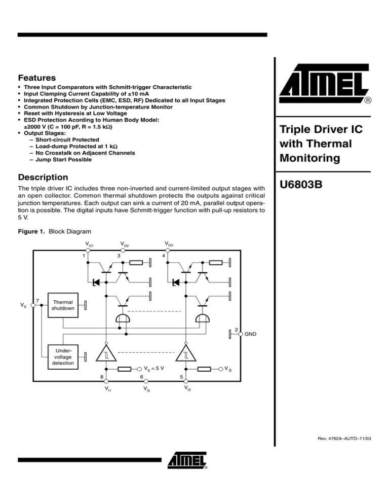
The triple driver IC includes three non-inverted and current-limited output stages with
an open collector. Common thermal shutdown protects the outputs against critical
junction temperatures. Each output can sink a current of 20 mA, parallel output operation is possible. The digital inputs have Schmitt-trigger function with pull-up resistors to
5 V.
U6803B
Figure 1. Block Diagram
VO1
1
VS
7
VO3
VO2
3
4
Thermal
shutdown
2
GND
Undervoltage
detection
VS = 5 V
8
6
VI1
VS
5
VI2
VI3
Rev. 4762A–AUTO–11/03
Pin Configuration
Figure 2. Pinning SO8
VO1
1
8
VI1
GND
2
7
VS
VO2
3
6
VI2
VO3
4
5
VI3
Pin Description
2
Pin
Symbol
Function
1
VO1
Output 1
2
GND
Ground
3
VO2
Output 2
4
VO3
Output 3
5
VI3
Input 3
6
VI2
Input 2
7
VS
Supply voltage 5 V
8
VI1
Input 1
U6803B
4762A–AUTO–11/03
U6803B
Basic Circuitry
The integrated circuit U6803B requires a stabilized supply voltage (VS = 5 V ±5%) to
comply with its electrical characteristics. An external buffer capacitor of C = 100 nF is
recommended. An integrated 14 V Zener diode between VS and ground protects the
supply pin.
All input stages are provided with an integrated 250 k W pull-up resistor and can be
directly connected to a microcontroller.
All output stages are open collectors, each capable of sinking 20 mA. Recommended
external components:
•
Pull-up resistor, R = 1 kW
•
Capacitor to GND, C = 470 pF, see Figure 3 on page 4
Functional Description
General
ON state: A low level at the input stage activates the corresponding output stage.
OFF state: The internal pull-up resistor provides a high level to the input comparator and
deactivates the output stage.
7 V Zener diodes between each input pin and GND are capable of ±10 mA clamping
currents without crosstalk on adjacent input stages.
A total clamping current of ±30 mA should be observed with respect to the power
dissipation.
Current Limitation of the
Output Stages and
Overtemperature
Shutdown
A temperature-dependent current limitation in the range of 25 to 100 mA protects the
stages in case of a short. Additionally, the chip temperature is monitored. For
TChip > 148°C, all outputs are disabled and automatically enabled with a hysteresis of
TChip > 5°C.
Transients and Load
Dump
An integrated 28 V Zener diode protects each output stage against transients and loaddump (Schaffner pulses). With the help of an external 1 kW resistor, the output transistor
is capable of handling the corresponding current which flows during each of these conditions. Apart from that, the outputs are short-circuit and overload protected.
Low-voltage Detection
When the supply voltage is switched on, a power-on reset pulse is generated internally
which disables all output stages until a defined supply-voltage level is reached. The
low-voltage detection is provided with a hysteresis of Vhyst = 0.5 V typically.
3
4762A–AUTO–11/03
Figure 3. Application Schematic
VS = 5 V
VBatt
Load
100 nF
VI1
Microcontroller
VI2
VI3
R
R
R
3 × 1 kΩ
VO1
U6803B
VO2
VO3
C
C
C
3 × 470 pF
Absolute Maximum Ratings
Stresses beyond those listed under “Absolute Maximum Ratings” may cause permanent damage to the device. This is a stress rating
only and functional operation of the device at these or any other conditions beyond those indicated in the operational sections of this
specification is not implied. Exposure to absolute maximum rating conditions for extended periods may affect device reliability.
Parameters
Symbol
Value
Unit
VS
7.0
V
Ambient temperature range
Tamb
-40 to +125
°C
Storage temperature range
Tstg
-50 to +150
°C
Tj
+150
°C
Symbol
Value
Unit
RthJA
160
K/W
Supply voltage
Maximum junction temperature
Thermal Resistance
Parameters
Junction ambient
4
U6803B
4762A–AUTO–11/03
U6803B
Electrical Characteristics
VS = 5 V ±5%, Tamb = 27°C, reference point pin 2 (GND), unless otherwise specified, see Figure 1 on page 1 and
Figure 3 on page 4
Parameters
Test Conditions
Symbol
Min.
VS
Typ.
Max.
Unit
4.75
5.25
V
IS
IS
0.8
7
3.2
13
mA
mA
VTH(ON)
VTH(OFF)
3.7
3.0
4.6
3.8
V
V
Low-voltage hysteresis
Vhyst
0.55
1.05
V
Temperature shutdown
TChip
140
149
°C
Temperature shutdown hysteresis
Thyst
5
VI
6.7
Supply, Pin 7
Supply voltage
Supply current
Inputs open
Inputs closed to GND
Low-voltage detection threshold
ON
OFF
°C
Input; Pins 5, 6, 8
Zener-diode protection voltage
II = 10 mA
Zener-diode clamping current
II
Pull-up resistor
RI
Switching threshold
OFF
ON
Hysteresis
170
250
8.5
V
±10
mA
305
kW
VI
VI
3.3
1.8
V
V
Vhyst
1.5
V
Output; Pins 1, 3, 4
Zener-diode protection voltage
IO = 10 mA
VO
26.5
Integrated capacitor
5
Leakage current
Saturation voltage
(IO = 20 mA)
Current limitation
Propagation delay
V
ILeak
2.5
µA
VSat
0.7
V
100
mA
5
µs
Ilimit
(470 pF, 1 kW, 20 V)
pF
td
25
5
4762A–AUTO–11/03
Ordering Information
Extended Type Number
Package
Remarks
U6803B-MFP
SO8
Tube
U6803B-MFPG3
SO8
Taped and reeled
Package Information
Package SO8
Dimensions in mm
5.2
4.8
5.00
4.85
3.7
1.4
0.25
0.10
0.4
1.27
6.15
5.85
3.81
8
0.2
3.8
5
technical drawings
according to DIN
specifications
1
6
4
U6803B
4762A–AUTO–11/03
Atmel Corporation
2325 Orchard Parkway
San Jose, CA 95131, USA
Tel: 1(408) 441-0311
Fax: 1(408) 487-2600
Regional Headquarters
Europe
Atmel Sarl
Route des Arsenaux 41
Case Postale 80
CH-1705 Fribourg
Switzerland
Tel: (41) 26-426-5555
Fax: (41) 26-426-5500
Asia
Room 1219
Chinachem Golden Plaza
77 Mody Road Tsimshatsui
East Kowloon
Hong Kong
Tel: (852) 2721-9778
Fax: (852) 2722-1369
Japan
9F, Tonetsu Shinkawa Bldg.
1-24-8 Shinkawa
Chuo-ku, Tokyo 104-0033
Japan
Tel: (81) 3-3523-3551
Fax: (81) 3-3523-7581
Atmel Operations
Memory
2325 Orchard Parkway
San Jose, CA 95131, USA
Tel: 1(408) 441-0311
Fax: 1(408) 436-4314
RF/Automotive
Theresienstrasse 2
Postfach 3535
74025 Heilbronn, Germany
Tel: (49) 71-31-67-0
Fax: (49) 71-31-67-2340
Microcontrollers
2325 Orchard Parkway
San Jose, CA 95131, USA
Tel: 1(408) 441-0311
Fax: 1(408) 436-4314
La Chantrerie
BP 70602
44306 Nantes Cedex 3, France
Tel: (33) 2-40-18-18-18
Fax: (33) 2-40-18-19-60
ASIC/ASSP/Smart Cards
1150 East Cheyenne Mtn. Blvd.
Colorado Springs, CO 80906, USA
Tel: 1(719) 576-3300
Fax: 1(719) 540-1759
Biometrics/Imaging/Hi-Rel MPU/
High Speed Converters/RF Datacom
Avenue de Rochepleine
BP 123
38521 Saint-Egreve Cedex, France
Tel: (33) 4-76-58-30-00
Fax: (33) 4-76-58-34-80
Zone Industrielle
13106 Rousset Cedex, France
Tel: (33) 4-42-53-60-00
Fax: (33) 4-42-53-60-01
1150 East Cheyenne Mtn. Blvd.
Colorado Springs, CO 80906, USA
Tel: 1(719) 576-3300
Fax: 1(719) 540-1759
Scottish Enterprise Technology Park
Maxwell Building
East Kilbride G75 0QR, Scotland
Tel: (44) 1355-803-000
Fax: (44) 1355-242-743
Literature Requests
www.atmel.com/literature
Disclaimer: Atmel Corporation makes no warranty for the use of its products, other than those expressly contained in the Company’s standard
warranty which is detailed in Atmel’s Terms and Conditions located on the Company’s web site. The Company assumes no responsibility for any
errors which may appear in this document, reserves the right to change devices or specifications detailed herein at any time without notice, and
does not make any commitment to update the information contained herein. No licenses to patents or other intellectual property of Atmel are
granted by the Company in connection with the sale of Atmel products, expressly or by implication. Atmel’s products are not authorized for use
as critical components in life support devices or systems.
© Atmel Corporation 2003. All rights reserved.
Atmel ® and combinations thereof are the registered trademarks of Atmel Corporation or its subsidiaries.
Other terms and product names may be the trademarks of others.
Printed on recycled paper.
4762A–AUTO–11/03

