Kilowatt Hot Swap/Circuit Breaker with Telemetry
advertisement

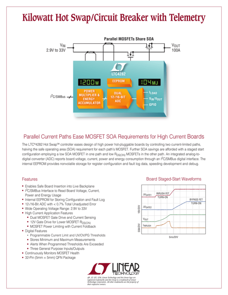
Kilowatt Hot Swap/Circuit Breaker with Telemetry Parallel MOSFETs Share SOA VOUT 100A VIN 2.9V to 33V LTC4282 EEPROM I2C/SMBus POWER MULTIPLIER & ENERGY ACCUMULATOR ILOAD DUAL 12-/16-BIT ADC VIN /VOUT GPIO Parallel Current Paths Ease MOSFET SOA Requirements for High Current Boards The LTC®4282 Hot SwapTM controller eases design of high power hot-pluggable boards by controlling two current-limited paths, halving the safe operating area (SOA) requirement for each path’s MOSFET. Further SOA savings are afforded with a staged start configuration employing a low SOA MOSFET in one path and low RDS(ON) MOSFETs in the other path. An integrated analog-todigital converter (ADC) reports board voltage, current, power and energy consumption through an I2C/SMBus digital interface. The internal EEPROM provides nonvolatile storage for register configuration and fault log data, speeding development and debug. Board Staged-Start Waveforms Features nn nn nn nn nn Enables Safe Board Insertion into Live Backplane I2C/SMBus Interface to Read Board Voltage, Current, Power and Energy Usage Internal EEPROM for Storing Configuration and Fault Log 12-/16-Bit ADC with < 0.7% Total Unadjusted Error Wide Operating Voltage Range: 2.9V to 33V High Current Application Features nn Dual MOSFET Gate Drive and Current Sensing nn 12V Gate Drive for Lower MOSFET R DS(ON) nn MOSFET Power Limiting with Current Foldback Digital Features nn ∆VGATE1 10V/DIV nn Programmable Current Limit and UV/OV/PG Thresholds Stores Minimum and Maximum Measurements nn Alerts When Programmed Thresholds Are Exceeded nn Three General Purpose Inputs/Outputs Continuously Monitors MOSFET Health 32-Pin (5mm × 5mm) QFN Package nn nn nn INRUSH FET TURN-ON ∆VGATE2 VOUT 50A/DIV nn L, LT, LTC, LTM, Linear Technology and the Linear logo are registered trademarks and Hot Swap is a trademark of Linear Technology Corporation. All other trademarks are the property of their respective owners. IINRUSH 5ms/DIV BYPASS FET TURN-ON LTC4282 Current Path Configurations Matched Paths Share SOA nn nn nn nn Recommended for Above 50A Applications MOSFETs Selected for High SOA and Low RDS(ON) Current Sharing Reduces MOSFET SOA Requirements by Half Long Fault Timer Rides Through Transients 0.5mΩ VIN Q2 0.5mΩ SENSE2+ VDD + Q1 SENSE1+ SENSE1– VOUT CL SENSE2– GATE1 GATE2 SOURCE LTC4282 TIMER GND 0.18µF High Stress Staged Start Rides Through Transients Q2 BYPASS nn nn nn nn Recommended for Below 50A Applications Medium RDS(ON), High SOA Q1 Handles Inrush, Load Surges and VIN Steps Low RDS(ON) Q2 Bypasses Q1 In Normal Operation Long Fault Timer Rides Through Transients 0.5mΩ VIN + Q1 STRESS 4.8k VDD SENSE1/2+ ADC+ 100Ω 1Ω SENSE1– ADC – VOUT CL SENSE2– GATE1 GATE2 SOURCE 24k FET Stress Signal Keeps Q2 Off GPIO2 LTC4282 TIMER GND 0.18µF 11ms Low Stress Staged Start for Lowest Cost nn nn nn nn Recommended for Above 50A Applications Small, Economical Q1 Trickle Charges Load Capacitance Low RDS(ON) Q2 Bypasses Q1 When GPIO1 Signals Power Good Short Fault Timer Disconnects on Overcurrent 0.5mΩ Q2 BYPASS VIN 10mΩ Q1 TRICKLE + 100Ω VOUT CL 30k 3.3µF VDD SENSE2+ SENSE1+ SENSE1– SENSE2– GATE1 GPIO1 LTC4282 TIMER GATE2 SOURCE 24k Gate RC Sets Inrush Output Low Signal Keeps Q2 Off GND 4.7nF 300µs www.linear.com/4282 n 1-800-4-LINEAR 0815


