AS1360
D a ta S he e t
1 . 5 µ A L o w - P o w e r, P o s i t i v e Vo l ta g e R e g u l a t o r
1 General Description
2 Key Features
The AS1360 low-power, positive voltage regulator was
designed to deliver up to 250mA while consuming only
1.5µA of quiescent current. The device is available in
fixed output voltages of 1.8, 2.1, 2.5, 3.0, 3.3, and 5.0V.
!
Low Quiescent Current: 1.5µA
!
Input Voltage Range: Up to 20V
The device features integrated short-circuit and overcurrent protection.
!
Low Dropout Voltage
- 250mV @ 100mA
- 400mV @ 200mA
The wide input voltage range, low-dropout voltage, and
high-accuracy output voltage makes the device perfectly
suited for 2- and 3-cell battery-powered and portable
applications.
The low dropout voltage (650mV) prolongs battery life
and allows high current in small applications when operated with minimum input-to-output voltage differentials.
The device features very stable output voltage (using
only 1µF tantalum or aluminum-electrolytic capacitors),
strict output voltage regulation tolerances (±0.5%), and
excellent line-regulation.
The AS1360 is available in a 3-pin SOT23 package.
!
Fixed Output Voltages: 1.8, 2.1, 2.5, 3.0, 3.3, 5.0V
!
High Output Current: 250mA (VOUT = 5.0V)
!
High-Accuracy Output Voltage: ±1.5%
!
Exceptional Line Regulation: 0.1%/V
!
Low Temperature Drift: ±100ppm/ºC
!
Integrated Short-Circuit and Overcurrent Protection
!
3-pin SOT23 Package
3 Applications
The device is ideal for mobile phones, PDAs, digital
cameras, smart battery packs, battery-powered alarms,
solar-powered instruments, intelligent instruments, CO2
and smoke detectors, CPU power supplies, and any battery-powered application.
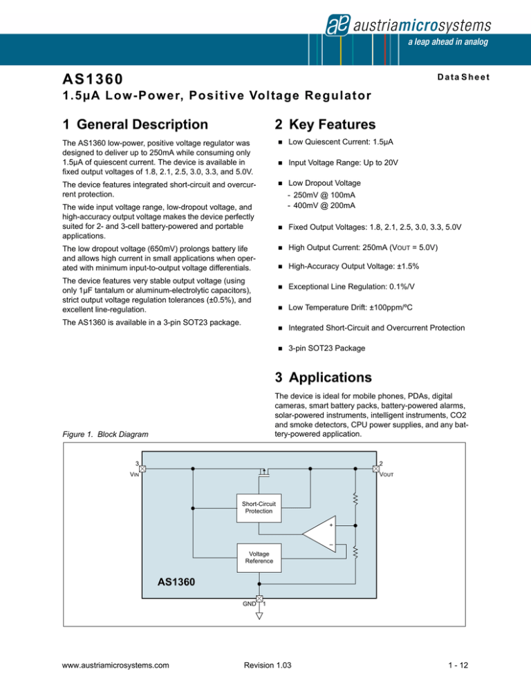
Figure 1. Block Diagram
3
2
VIN
VOUT
Short-Circuit
Protection
+
–
Voltage
Reference
AS1360
GND
www.austriamicrosystems.com
1
Revision 1.03
1 - 12
AS1360
Data Sheet - P i n o u t a n d P a c k a g i n g
4 Pinout and Packaging
Pin Assignments
Figure 2. Pin Assignments (Top View)
GND
1
AS1360
VOUT
3
VIN
2
3-pin SOT23
Pin Descriptions
Table 1. Pin Descriptions
Pin Number
1
2
3
Pin Name
Description
GND
Ground. This pin should be connected to the negative side of the output and
the negative terminal of the input capacitor. No high-current flows out of this
pin, only bias current (1.5µA, typ).
Note: Voltage drops between this pin and the negative side of the load
should be minimized.
VOUT
Regulated Output Voltage. This pin should be connected to the positive
side of the load and the positive terminal of the output capacitor. Current
flowing out of this pin is equivalent DC load current.
Note: The positive side of the output capacitor should be mounted as close
as is practical to this pin.
VIN
Unregulated Input Voltage. This pin should be connected to the positive
terminal of the input capacitor.
Note: The input capacitor should be mounted as close as is practical to this
pin.
www.austriamicrosystems.com
Revision 1.03
2 - 12
AS1360
Data Sheet - A b s o l u t e M a x i m u m R a t i n g s
5 Absolute Maximum Ratings
Stresses beyond those listed in Table 2 may cause permanent damage to the device. These are stress ratings only,
and functional operation of the device at these or any other conditions beyond those indicated in Section 6 Electrical
Characteristics on page 4 is not implied. Exposure to absolute maximum rating conditions for extended periods may
affect device reliability.
Table 2. Absolute Maximum Ratings
Parameter
Min
Max
Units
Input Voltage
+30
V
Continuous Output Current
PD/
(VIN - VOUT)
mA
Peak Output Current
500
mA
Output Voltage
- 0.3V
VIN + 0.3V
or +7V
V
Minimum of the two values
230
ºC/W
Typical FR4, 4-layer application
Operating Temperature Range
-40
+85
ºC
Storage Temperature Range
-40
+125
ºC
Thermal Resistance ΘJA
Electrostatic Discharge (ESD)
Protection Level
Package Body Temperature
www.austriamicrosystems.com
1
+260
Comments
kV
HBM - Norm: MIL 883 E methode 3015
ºC
The reflow peak soldering temperature
(body temperature) specified is in
compliance with IPC/JEDEC J-STD-020C
“Moisture/ Reflow Sensitivity
Classification for Non-Hermetic Solid
State Surface Mount Devices”.
Revision 1.03
3 - 12
AS1360
Data Sheet - E l e c t r i c a l C h a r a c t e r i s t i c s
6 Electrical Characteristics
TAMB = +25ºC (unless otherwise specified).
Table 3. Electrical Characteristics
Symbol
VIN
Parameter
Condition
Min
Input Voltage
1
Typ
Max
Unit
20
V
VOUTNOM VOUTNOM VOUTNOM
IOUT = 40mA ,
- 1.5%
± 0.5%
+ 1.5%
IOUT = 15mA if VOUT = 1.8V
VOUT = 5.0V
250
(VIN = VOUTNOM + 1.0V)
VOUT = 3.3V
150
Maximum Output
150
VOUT = 3.0V
IOUT(MAX)
Current
125
VOUT = 2.5V
115
VOUT = 2.1V
110
VOUT = 1.8V
VOUT = 5.0V, 1mA ≤ IOUT ≤ 100mA
-1.60
±0.8
+1.60
VOUT = 3.3V, 1mA ≤ IOUT ≤ 80mA
-2.72
±1.3
+2.72
-3.00
±1.5
+3.00
VOUT = 3.0V, 1mA ≤ IOUT ≤ 80mA
2
ΔVOUT/VOUT
Load Regulation
-3.60
±1.8
+3.60
VOUT = 2.5V, 1mA ≤ IOUT ≤ 60mA
VOUT = 2.1V, 1mA ≤ IOUT ≤ 40mA
-2.60
±1.6
+2.60
-1.60
±0.8
+1.60
VOUT = 1.8V, 1mA ≤ IOUT ≤ 30mA
ΔVOUT x 100/
I
OUT = 40mA,
Line Regulation
0.1
0.25
ΔVIN x VOUT
(VOUTNOM +1.0) ≤ VIN ≤ 10.0V
400
630
IOUT = 200mA, VOUTNOM = 5.0V
IOUT = 160mA, VOUTNOM = 3.3V
400
700
400
700
IOUT = 160mA, VOUTNOM = 3.0V
VIN - VOUT
Dropout Voltage
IOUT = 120mA, VOUTNOM = 2.5V
400
700
200
500
IOUT = 60mA, VOUTNOM = 2.1V
180
300
IOUT = 20mA, VOUTNOM = 1.8V
IQ
Input Quiescent Current
VIN = VOUTNOM +1.0V
1.5
3.0
Temperature Coefficient
IOUT = 40mA,
TCVOUT
±100
3
-40ºC ≤ TAMB ≤ +85ºC
of VOUT
10% VOUTNOM to 90% VOUTNOM,
tR
Output Rise Time
VIN = 0V to VOUTNOM + 1V,
150
RLOAD = 25Ω resistive
VOUT
Output Voltage
V
mA
%
%/V
mV
µA
ppm/
ºC
µs
1. VOUTNOM is the nominal device output voltage.
2. Measured at a constant junction temperature using low duty cycle pulse testing.
6
3. TCVOUT = (VOH - VOL) x 10 /(VOUTNOM x Temperature).
Where:
VOH is the highest voltage measured over the device temperature range.
VOL is the lowest voltage over the device temperature range.
www.austriamicrosystems.com
Revision 1.03
4 - 12
AS1360
Data Sheet - Ty p i c a l O p e r a t i n g C h a r a c t e r i s t i c s
7 Typical Operating Characteristics
VOUT = 3.3V, ILOAD = 100µA, VIN = 4.3V, CIN 1µF (tantalum), COUT = 1µF (tantalum), TAMB = +25ºC (unless otherwise
specified).
Figure 4. Supply Current vs. Load Current;
1.9
1.9
1.8
1.8
1.7
Supply Current (µA) .
Supply Current (µA) .
Figure 3. Supply Current vs. Input Voltage;
85°C
1.6
1.5
25°C
1.4
0°C
1.3
1.2
85°C
1.7
1.6
25°C
1.5
0°C
1.4
1.3
-40°C
1.2
-40°C
1.1
1.1
4
5
6
7
8
9
10
0
25
50
Input Voltage (V)
Figure 6. Output Voltage vs. Input Voltage;
1.9
3.312
1.8
3.31
Output Voltage (V) .
Supply Current (µA) .
Figure 5. Supply Current vs. Temperature;
1.7
1.6
1.5
1.4
1.3
1.2
25°C
0°C
3.308
3.306
3.304
3.302
-40°C
3.3
85°C
3.298
1.1
-40 -20
3.296
0
20 40 60 80 100 120 140
4
5
6
Temperature (°C)
7
8
9
10
Input Voltage (V)
Figure 7. Output Voltage vs. Load Current,
Figure 8. Dropout Voltage vs. Load Current;
3.31
700
85°C
Dropout Voltage (mV) .
25°C
3.3
Output Voltage (V) .
75 100 125 150 175 200
Load Current (mA)
3.29
-40°C
3.28
0°C
3.27
3.26
3.25
600
500
400
25°C
0°C
300
200
-40°C
100
3.24
85°C
3.23
0
0
10
20
30
40
50
60
70
80
0
Load Current (mA)
www.austriamicrosystems.com
20
40
60
80 100 120 140 160
Load Current (mA)
Revision 1.03
5 - 12
AS1360
Data Sheet - Ty p i c a l O p e r a t i n g C h a r a c t e r i s t i c s
Figure 9. Load Regulation vs. Temperature,
Figure 10. Line Regulation vs. Temperature;
2.5
0.2
1mA / 10mA
0
.
VIN = 10V
2.1
1.9
1.7
1.5
VIN = 6V
1.1
VIN = 4.3V
0.9
40mA
-0.2
-0.4
-0.6
-0.8
0.5
-40
-15
10
35
60
85
150mA
-1
0.7
-1.2
-40
Temperature (°C)
-15
10
60
85
Figure 12. Startup Delay;
50µs/Div
1V/Div
VOUT
500mV/Div
VIN
Figure 11. Startup Rise Time;
VOUT
35
Temperature (°C)
2V/Div
1.3
Line Regulation (%/V)
Load Regulation (%)
.
2.3
10ms/Div
Note: All graphs where measured without additional heat sinks, with the SOT23 package mounted on a 4-layer PCB.
Adding additional heat sinks will improve performance in high temperature enviroment.
www.austriamicrosystems.com
Revision 1.03
6 - 12
AS1360
Data Sheet - D e t a i l e d D e s c r i p t i o n
8 Detailed Description
The AS1360 is a low-power, positive voltage regulator designed in such a way that the supply current is independent
from the load current. The device regulates the output by comparing the output voltage to an internally generated reference voltage.
The device is available in fixed output voltages of 1.8, 2.5, 3.0, 3.3, and 5.0V. Fixed output voltages are generated
using the internal resistor divider network (see Figure 1 on page 1).
Short Circuit/Overcurrent Protection
The AS1360 monitors current flow through the p-channel MOSFET. In short-circuit or overcurrent conditions, the integrated short-circuit protection circuitry will limit output current.
Note: Thermal Dissipation according to Absolute Maximum Ratings on page 3 must be considered.
www.austriamicrosystems.com
Revision 1.03
7 - 12
AS1360
Data Sheet - A p p l i c a t i o n I n f o r m a t i o n
9 Application Information
Figure 13. Typical Application Diagram
+9V
Alkaline
Battery
3
VIN
CIN
1µF
AS1360
VOUT
*
VOUT = 3.3V
COUT
1µF
GND
*
2
*
1
Tantalum Capacitor
Power Dissipation
Power dissipation (PD) of the AS1360 is the sum of the power dissipated by the p-channel MOSFET and the quiescent
current required to bias the internal voltage reference and the internal power amplifier, and is calculated as:
PD (P-Channel MOSFET) = (VIN - VOUT)IOUT
(EQ 1)
Internal power dissipation as a result of the bias current for the internal voltage reference and the error amplifier is calculated as:
PD (Bias) = VINIGND
(EQ 2)
Total AS1360 power dissipation is calculated as:
PD(Total) = PD (P-Channel MOSFET) + PD (Bias)
(EQ 3)
The internal quiescent bias current (2µA, typ) is such that the PD(Bias) term of (EQ 3) can be disregarded and the
maximum power dissipation can be estimated using VIN(MAX) and VOUT(MIN) to obtain a maximum voltage differential
between VIN and VOUT, and multiplying the maximum voltage differential by the maximum output current:
PD = (VIN(MAX)VOUT(MIN))IOUT(MAX)
(EQ 4)
Where:
VIN = 3.3 to 4.1V
VOUT = 3.0V ±2%
IOUT = 1 to 100mA
TAMB(MAX) = 55ºC
PMAX = (4.1V - (3.0V x 0.98)) x 100mA = 116.0mW
Junction Temperature
The AS1360 junction temperature (TJ) can be determined by first calculating the thermal resistance from junction temperature-to-ambient temperature.
Note: Thermal resistance is estimated to be the junction temperature-to-air temperature RΦJA, and is approximately
230°C/W or 335ºC/W (when mounted on 1 square inch of copper). RΦJA will vary depending on PCB layout,
air-flow and application specific conditions.
The AS1360 junction temperature is determined by calculating the rise in TJ above TAMB, and then adding the increase
of TAMB:
TJ = PD(MAX) x RΦJA + TAMB
(EQ 5)
From (EQ 5), the value of TJ can be calculated as:
TJ = 116.0mW x 230ºC/W + 55ºC
Therefore:
TJ = 81.68ºC
www.austriamicrosystems.com
Revision 1.03
8 - 12
AS1360
Data Sheet - A p p l i c a t i o n I n f o r m a t i o n
External Component Selection
Input Capacitor
In applications where input impedance is approximately 10Ω, a 1µF capacitor is sufficient for CIN (see Figure 13 on
page 8).
In cases where the AS1360 is operated from a battery, or when there is significant distance between the input source
to the AS1360, larger values for CIN may be required for output stability.
Note: For values of COUT > 1µF, the value of CIN should be increased to prevent high source-impedance oscillations.
Output Capacitor
In most applications for the AS1360, a 1µF capacitor (ESR > 0.1Ω/< 5Ω, fRES > 1MHz) is sufficient for COUT (see Figure 13 on page 8).
For improved power supply noise rejection and device transient response, larger values can be used for COUT.
Note: For values of COUT > 1µF, the input impedance must not be so large that it causes high-input impedance oscillations.
www.austriamicrosystems.com
Revision 1.03
9 - 12
AS1360
Data Sheet - P a c k a g e D r a w i n g s a n d M a r k i n g s
10 Package Drawings and Markings
The device is available in an 3-pin SOT23 package.
Figure 14. 3-pin SOT23 Package
Notes:
1. Lead coplanarity should be 0 to 0.10mm (.004”) max.
2. Package surfacing:
a. Top: matte (charmilles #18- 30).
b. All sides: matte (charmilles #18- 30).
c. Bottom: smooth or matte (charmilles #18- 30).
3. All dimensions excluding mold flashes and end flash from the
package body shall not exceed 0.25mm (.010”) per side (D).
4. Details of pin #1 identifier are optional but must be located
within the zone indicated.
5. Dimensions are in millimeters.
www.austriamicrosystems.com
Revision 1.03
Symbol
A
A1
B
C
D
E
e
e1
H
L
A
S
Min
0.89
0.013
0.37
0.085
2.80
1.20
0.89
1.78
2.10
Max
1.12
0.100
0.51
0.18
3.04
1.40
1.03
2.05
2.64
0.55ref
0.89
0.45
1.12
0.60
10 - 12
AS1360
Data Sheet - O r d e r i n g I n f o r m a t i o n
11 Ordering Information
The device is available as the standard products shown in Table 4.
Table 4. Ordering Information
Model
Marking
Description
Delivery Form
Package
AS1360-18-T
ASKD
HV low-quiescent current LDO, 1.8V
Tape and Reel
3-pin SOT23
AS1360-21-T
ASRO
HV low-quiescent current LDO, 2.1V
Tape and Reel
3-pin SOT23
AS1360-25-T
ASKE
HV low-quiescent current LDO, 2.5V
Tape and Reel
3-pin SOT23
AS1360-30-T
ASKF
HV low-quiescent current LDO, 3.0V
Tape and Reel
3-pin SOT23
AS1360-33-T
ASKG
HV low-quiescent current LDO, 3.3V
Tape and Reel
3-pin SOT23
AS1360-50-T
ASKH
HV low-quiescent current LDO, 5.0V
Tape and Reel
3-pin SOT23
All devices are RoHS compliant and free of halogene substances.
www.austriamicrosystems.com
Revision 1.03
11 - 12
AS1360
Data Sheet
Copyrights
Copyright © 1997-2009, austriamicrosystems AG, Schloss Premstaetten, 8141 Unterpremstaetten, Austria-Europe.
Trademarks Registered ®. All rights reserved. The material herein may not be reproduced, adapted, merged, translated, stored, or used without the prior written consent of the copyright owner.
All products and companies mentioned are trademarks or registered trademarks of their respective companies.
Disclaimer
Devices sold by austriamicrosystems AG are covered by the warranty and patent indemnification provisions appearing
in its Term of Sale. austriamicrosystems AG makes no warranty, express, statutory, implied, or by description regarding
the information set forth herein or regarding the freedom of the described devices from patent infringement. austriamicrosystems AG reserves the right to change specifications and prices at any time and without notice. Therefore,
prior to designing this product into a system, it is necessary to check with austriamicrosystems AG for current information. This product is intended for use in normal commercial applications. Applications requiring extended temperature
range, unusual environmental requirements, or high reliability applications, such as military, medical life-support or lifesustaining equipment are specifically not recommended without additional processing by austriamicrosystems AG for
each application. For shipments of less than 100 parts the manufacturing flow might show deviations from the standard
production flow, such as test flow or test location.
The information furnished here by austriamicrosystems AG is believed to be correct and accurate. However,
austriamicrosystems AG shall not be liable to recipient or any third party for any damages, including but not limited to
personal injury, property damage, loss of profits, loss of use, interruption of business or indirect, special, incidental or
consequential damages, of any kind, in connection with or arising out of the furnishing, performance or use of the technical data herein. No obligation or liability to recipient or any third party shall arise or flow out of
austriamicrosystems AG rendering of technical or other services.
Contact Information
Headquarters
austriamicrosystems AG
A-8141 Schloss Premstaetten, Austria
Tel: +43 (0) 3136 500 0
Fax: +43 (0) 3136 525 01
For Sales Offices, Distributors and Representatives, please visit:
http://www.austriamicrosystems.com/contact-us
www.austriamicrosystems.com
Revision 1.03
12 - 12


