User Guide UG062
ISL7823xEVAL2Z Evaluation Board User Guide
Description
Key Features
The ISL78233EVAL2Z, ISL78234EVAL2Z and ISL78235EVAL2Z
evaluation boards are used to demonstrate the performance of
the ISL78233, ISL78234 and ISL78235 low quiescent current,
high efficiency synchronous buck regulators. The evaluation
boards are intended for use by customers with requirements for
point-of-load automotive applications with 2.7V to 5.5V input
supply voltage, output voltages down to 0.8V and up to a 5A
output current.
• 2.7V to 5.5V input voltage range
• Synchronous buck regulator up to 95% efficiency
• 1% reference accuracy over temperature
• Resistor adjustable frequency from 500kHz to 4MHz;
Default set to 2MHz
• External synchronization from 1MHz to 4MHz
• 100ns maximum phase minimum on time allows wide
output regulation operating at 2MHz
The ISL78233, ISL78234 and ISL78235 are offered in a
5x5mm 16 Ld Wettable Flank QFN (WFQFN) package with
0.9mm maximum height.
• Internal soft-start set to 1ms; adjustable with external
soft-start capacitor
Specifications
PART
NUMBER
IOUT
(MAX)
(A)
ISL78235
5
ISL78234
4
ISL78233
3
fSW RANGE
(MHz)
• Over-temperature, overcurrent, overvoltage and negative
overcurrent protection
VIN
VOUT
RANGE RANGE
(V)
(V)
References
PART SIZE
(mm)
• ISL78235 Datasheet
Programmable
1MHz to 4MHz
2.7 to
5.5
0.8 to
5.5
• ISL78233, ISL78234 Datasheet
5x5
Ordering Information
PART NUMBER
PCB SPECIFICATION
Board Dimension: 2.025inx2.725in
# of Layers: 4
FR-4 Thickness: 1.57mm
Copper Weight: 2oz.
ISL78235EVAL2Z
Evaluation Board for 5A Synchronous Buck
ISL78235
ISL78234EVAL2Z
Evaluation Board for 4A Synchronous Buck
ISL78234
ISL78233EVAL2Z
Evaluation Board for 3A Synchronous Buck
ISL78233
NOTES:
1. The evaluation board default VOUT = 1.8V.
2. The evaluation board default fSW = 2MHz.
16
VIN
PHASE
14
11
*ISL78235
3
10
SYNC 4
9
8
COMP
7
SS
FS
EN
6
5A LOAD
DSP, FPGA
13
12
5
VOUT
COUT
1
VDD 2
PG
15
PHASE
VIN
CIN
PHASE
L
2.7V TO 5.5V
DESCRIPTION
PGND
PGND
SGND
FB
*Pin Compatible
ISL78233 - 3A BUCK
ISL78234 - 4A BUCK
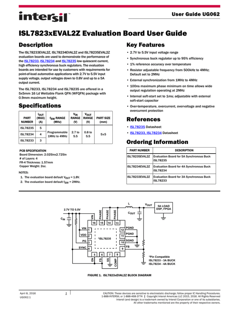
FIGURE 1. ISL7823xEVAL2Z BLOCK DIAGRAM
April 8, 2016
UG062.1
1
CAUTION: These devices are sensitive to electrostatic discharge; follow proper IC Handling Procedures.
1-888-INTERSIL or 1-888-468-3774 | Copyright Intersil Americas LLC 2015, 2016. All Rights Reserved
Intersil (and design) is a trademark owned by Intersil Corporation or one of its subsidiaries.
All other trademarks mentioned are the property of their respective owners.
User Guide UG062
Recommended Equipment
Frequency Control
The following equipment is recommended to perform testing:
• 0V to 5V power supply with 10A source current capability
• Electronic load capable of sinking current up to 10A
• Digital Multimeters (DMMs)
• 500MHz quad-trace oscilloscope
The ISL78233, ISL78234 and ISL78235 have an FS pin that
controls the frequency of operation. Programmable frequency
allows for optimization between efficiency and external
component size. Default switching frequency is 2MHz when FS is
tied to VIN (R6 = 0). By removing R6 and changing the value of
R4, the switching frequency can be changed from 500kHz to
4MHz according to Equation 2:
220 10 3
R 4 k = ------------------------------ – 14
f OSC kHz
• Signal generator for EN and/or SYNC pins
Quick Setup Guide
1. Ensure that the circuit is correctly connected to the supply and
loads prior to applying any power.
2. Connect the bias supply to VIN, the plus terminal to VIN (P4)
and the negative return to PGND (P5).
3. Connect the output load to VOUT, the plus terminal to VOUT
(P3) and the negative return to PGND (P7).
4. Verify that SW2 is in the proper position for PFM or PWM.
5. Verify that the position is ON for SW1.
6. Turn on the power supply and set for 2.7V to 5.0V.
(EQ. 2)
Please refer to the ISL78235, ISL78233, ISL78234 datasheets
for more details.
Soft-Start Control
The ISL78233, ISL78234 and ISL78235 have an SS pin that
controls the soft start-up time. Short the SS pin to SGND for
internal soft-start (approximately 1ms). Populate a capacitor at
C6 to adjust the soft-start time. This capacitor, along with an
internal 2.1µA current source sets the soft-start interval of the
converter, tSS.
C6 F = 3.5 t SS s
7. Verify the output voltage is 1.8V for VOUT.
Functional Description
The ISL78233EVAL2Z, ISL78234EVAL2Z and ISL78235EVAL2Z
evaluation boards are used to demonstrate the performance of the
ISL78233, ISL78234 and ISL78235 low quiescent current, high
efficiency synchronous buck regulators. The evaluation boards are
intended for use by customers with requirements for point-of-load
automotive applications with 2.7V to 5.5V input supply voltage,
output voltages down to 0.8V and up to a 5A output current. The
ISL78233, ISL78234 and ISL78235 are offered in a 5x5mm
16 Ld Wettable Flank QFN (WFQFN) package with 0.9mm
maximum height.
The schematics for the evaluation boards are shown in Figure 4
on page 5. The evaluation boards include all components to
easily evaluate the performance of the buck regulator. Hardware
included on the evaluation boards allows the user to operate the
following functions: Toggle switch for Enable/Disable, Toggle
switch for PFM/forced PWM operation and test points for
monitoring the switching node and output voltage.
Operating Voltage Range
The ISL78233EVAL2Z, ISL78234EVAL2Z and ISL78235EVAL2Z
evaluation boards are designed to operate with 2.7V to 5.5V VIN and
the outputs are preset to 1.8V for VOUT. The output voltage can
be adjusted from 0.8V to 3.3V. The output voltage programming
resistor, R2, depends on the desired output voltage of the
regulator. It is recommended to have R3 set to 100kΩ. The value
for R2 is typically between 66kΩ and 450kΩ and is determined in
Equation 1.
(EQ. 3)
C6 should be less than 33nF to insure proper soft-start reset after
a fault condition. The ISL78233EVAL2Z, ISL78234EVAL2Z and
ISL78235EVAL2Z have a default 33nF on the board for a ~10ms
soft-start time.
Control Switches for EN and SYNC
The evaluation boards contain switches SW1 and SW2 for control
of the EN and SYNC pin. Table 1 details this function.
TABLE 1. SWITCH SETTINGS
SW1
ENABLE
FUNCTION
1 (LEFT)
OFF
Disable IC
3 (RIGHT)
ON
Enable IC
SW2
SYNC
1 (LEFT)
PFM
Skip mode at light load
3 (RIGHT)
PWM
Fixed PWM frequency at light
load
FUNCTION
Power Inductor
The evaluation boards contain a 0.68µH output power inductor. It
has a 13.5A saturation current that is able to handle the peak
current limit of the IC. The inductor is chosen to optimize
performance for VIN = 5V, VOUT = 1.8V at 2MHz switching
frequency for up to 5A output currents.
(EQ. 1)
R 2 = R 3 VO VFB – 1
For faster transient response performance, add 10pF to 22pF in
parallel to R2. Check loop compensation analysis to insure
optimum performance before use of capacitance.
Submit Document Feedback
2
UG062.1
April 8, 2016
User Guide UG062
FIGURE 2. ISL78235EVAL2Z TOP SIDE
FIGURE 3. ISL78235EVAL2Z BOTTOM SIDE
Submit Document Feedback
3
UG062.1
April 8, 2016
User Guide UG062
Internal vs External Compensation
The ISL78233, ISL78234 and ISL78235 feature an internal
compensation network on the output of the error amplifier. The
internal compensation simplifies design by reducing external
components while stabilizing the regulator under transient load
response. To use an internal compensation network, tie the
COMP pin to VDD.
The restriction of an internal compensation network is that it
does not provide flexibility to optimize the compensation network
for conditions when additional output capacitance is needed to
minimize output overshoot from fast transient loading. The
added capacitance affects the stability and response of the
feedback loop. The internal compensation network is well suited
for a wide range of switching frequencies and load di/dt
transients, however, if the feedback network needs to be better
optimized for the application, external compensation should be
used. When the COMP pin is not connected to VDD, an RC
network from the COMP pin to GND is used to provide the
external compensation.
PCB Layout Recommendation
The PCB layout is a very important converter design step to make
sure the designed converter works well. For ISL78233, ISL78234
and ISL78235, the power loop is composed of the output inductor
Lo, the output capacitor (COUT), the PHASE pins and the PGND
pins. It is necessary to make the power loop as small as possible
and the connecting traces among them should be direct, short
and wide. The switching node of the converter (PHASE pins) and
the traces connected to the node are noisy. Keep the voltage
feedback trace away from these noisy traces. The input capacitor
should be placed as close as possible to the VIN/VDD and GND
pin. The ground of input and output capacitors should be
connected as close as possible. The heat of the IC is mainly
dissipated through the thermal pad. Maximizing the copper area
connected to the thermal pad is preferable. In addition, a solid
ground plane is helpful for better EMI performance. Refer to
TB389 for via placement on the copper area of the PCB
underneath the thermal pad for optimal thermal performance.
For more information on the specification of the internal
compensation network and designing for stability, refer to the
ISL78235, ISL78233, ISL78234 datasheets for more details.
Submit Document Feedback
4
UG062.1
April 8, 2016
User Guide UG062
ISL7823xEVAL2Z Schematics
NOTES:
3. ISL78235EVAL2Z schematics are shown.
4. ISL78233EVAL2Z and ISL78234EVAL2Z schematics are equivalent.
FIGURE 4. ISL7823xEVAL2Z SCHEMATICS
Submit Document Feedback
5
UG062.1
April 8, 2016
Submit Document Feedback
Bill Of Materials
MANUFACTURER
PART
6
REFERENCE
DESIGNATOR
ISL78233AARZ or
ISL78234AARZ or
ISL78235AARZ
1
U1
0603ZC104K4T2A
1
C5
131-4353-00
2
J1, J2
2N7002
1
Q1
AUTO-CAP-SM0603-OPEN
1
C9
DNP
AUTO-RES-SM0603-DNP
3
R10, R12, R14
DNP
C0603C332K4RACAUTO
1
C6
3300pF
10%
CGA3E2COG1H221J080AA
1
C7
220pF
5%
CRCW06030000Z0EA
1
R6
0
1%
CRCW0603100KFKEA
1
R3
100k
CRCW0603200KFKEA
4
R2, R8, R11, R13
CRCW060320R0FKEA
1
CRCW06032K00FKEA
VALUE
TOL.
VOLTAGE
POWER
PACKAGE
TYPE
WFQFN16
DESCRIPTION
MANUFACTURER
3A, 4A, 5A Compact Synchronous Buck Regulator
INTERSIL
Ceramic Chip Cap (Automotive AEC-Q200)
AVX
CONN
Scope Probe Test Point PCB Mount
TEKTRONIX
SOT23
N-Channel EMF Effect Transistor
FAIRCHILD
603
Ceramic Chip Cap (Automotive AEC-Q200)
Generic
603
Film Chip Resistor (Automotive AEC-Q200)
Generic
16V
603
Ceramic Chip Cap (Automotive AEC-Q200)
Kemet
50V
603
Ceramic Chip Cap (Automotive AEC-Q200)
TDK
1/10W
603
Film Chip Resistor (Automotive AEC-Q200)
VISHAY
1%
1/10W
603
Film Chip Resistor (Automotive AEC-Q200)
VISHAY
200k
1%
1/10W
603
Film Chip Resistor (Automotive AEC-Q200)
VISHAY
R7
20
1%
1/10W
603
Film Chip Resistor (Automotive AEC-Q200)
VISHAY
1
R9
2k
1%
1/10W
603
Film Chip Resistor (Automotive AEC-Q200)
VISHAY
CRCW060369K8FKEA
1
R5
69.8k
1%
1/10W
603
Film Chip Resistor (Automotive AEC-Q200)
VISHAY
CRCW060395K3FKEA
1
R4
95.3k
1%
1/10W
603
Film Chip Resistor (Automotive AEC-Q200)
VISHAY
GCM1885C1H220JA16D
1
C8
22pF
5%
50V
603
Ceramic Chip Cap (Automotive AEC-Q200)
Murata
GCM31CR71A226KE
2
C3, C4
22µF
10%
10V
1206
Ceramic Chip Cap (Automotive AEC-Q200)
Murata
GCM32ER71A226KE12L
2
C1, C2
22µF
10%
10V
1210
Ceramic Chip Cap (Automotive AEC-Q200)
Murata
GT11MSCKE
2
SW1, SW2
SMT
SPDT On-None-On SMT Ultraminature Toggle Switch
C&K
H1082-OPEN
2
C14, C15
DNP
1210
Ceramic Chip Cap
GENERIC
H2511-00100-1/16W1
1
R1
10
1%
1/16W
603
Thick Film Chip Resistor
GENERIC
IHLP-2020CZ-ER-R68-M-01
1
L1
0.68µH
20%
10.2A
SMD-S
Low Profile High Current Inductor
VISHAY
JMK325B7476KMHTR
4
C10-C13
47µF
10%
1210
Ceramic Chip Cap (Automotive AEC-Q200)
Taiyo Yuden
LTST-C170CKT
1
D1
SMD
AlGaAs on GaAs Red LED
LITEON
0.10µF
10%
10V
6.3V
603
User Guide UG062
QTY
UG062.1
April 8, 2016
User Guide UG062
ISL7823xEVAL2Z Board Layout
FIGURE 5. TOP LAYER SILKSCREEN
FIGURE 6. BOTTOM LAYER SILKSCREEN
NOTES:
5. ISL78233 board silkscreen name is ISL78233EVAL2Z
6. ISL78234 board silkscreen name is ISL78234EVAL2Z
Submit Document Feedback
7
UG062.1
April 8, 2016
User Guide UG062
ISL7823xEVAL2Z Board Layout
(Continued)
FIGURE 7. LAYER 1 PCB
FIGURE 8. LAYER 2 PCB
FIGURE 9. LAYER 3 PCB
FIGURE 10. LAYER 4 PCB
Submit Document Feedback
8
UG062.1
April 8, 2016
User Guide UG062
Typical Performance Curves
100
2.5
3.3VOUT
90
2.5VOUT
POWER DISSIPATION (W)
EFFICIENCY (%)
80
1.8VOUT
1.5VOUT
70
1.2VOUT
60
3.3VOUT
2.0
2.5VOUT
1.8VOUT
1.5
1.5VOUT
1.0
0.5
50
1.2VOUT
0
40
0
0.5
1.0
1.5
2.0
2.5
3.0
3.5
4.0
4.5
0
5.0
0.5
1.0
2.5
3.0
POWER DISSIPATION (W)
80
70
1.5VOUT
1.2VOUT
1.0VOUT
60
50
40
0
0.5
1.0
1.5
2.0
2.5
3.0
3.5
4.0
5.0
1.5
2.5VOUT
1.0
1.0VOUT
5.0
1.2VOUT
0.5
0
4.5
FIGURE 13. EFFICIENCY vs LOAD (3VIN; SYNC = VDD)
COUT = 4x47µF
RCOMP = 332kΩ
CCOMP = 150pF
ILOAD 2A/DIV
4.5
1.5VOUT
0
0.5
OUTPUT LOAD (A)
VOUT 50mV/DIV AC COUPLED
4.0
1.8VOUT
2.0
1.8VOUT
3.5
2.5
2.5VOUT
90
EFFICIENCY (%)
2.0
FIGURE 12. POWER DISSIPATION vs LOAD (5VIN; SYNC = VDD)
FIGURE 11. EFFICIENCY vs LOAD (5VIN; SYNC = VDD)
100
1.5
OUTPUT LOAD (A)
OUTPUT LOAD (A)
400µs/DIV
FIGURE 15. LOAD TRANSIENT 0A TO 5A; 0.5A/µs (SYNC = GND)
1.0
1.5
2.0
2.5
3.0
OUTPUT LOAD (A)
3.5
4.0
4.5
5.0
FIGURE 14. POWER DISSIPATION vs LOAD (3VIN; SYNC = VDD)
VOUT 50mV/DIV AC COUPLED
COUT = 4x47µF
RCOMP = 332kΩ
CCOMP = 150pF
ILOAD 2A/DIV
400µs/DIV
FIGURE 16. LOAD TRANSIENT 0A TO 5A; 0.5A/µs (SYNC = VDD)
Intersil Corporation reserves the right to make changes in circuit design, software and/or specifications at any time without notice. Accordingly, the reader is
cautioned to verify that the document is current before proceeding.
For information regarding Intersil Corporation and its products, see www.intersil.com
Submit Document Feedback
9
UG062.1
April 8, 2016

