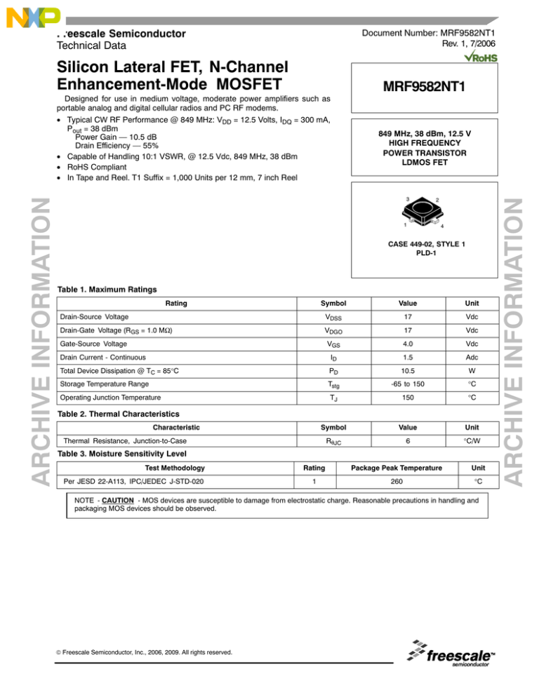
Document Number: MRF9582NT1
Rev. 1, 7/2006
Freescale Semiconductor
Technical Data
Silicon Lateral FET, N-Channel
Enhancement-Mode MOSFET
MRF9582NT1
849 MHz, 38 dBm, 12.5 V
HIGH FREQUENCY
POWER TRANSISTOR
LDMOS FET
3
1
ARCHIVE INFORMATION
ARCHIVE INFORMATION
Designed for use in medium voltage, moderate power amplifiers such as
portable analog and digital cellular radios and PC RF modems.
• Typical CW RF Performance @ 849 MHz: VDD = 12.5 Volts, IDQ = 300 mA,
Pout = 38 dBm
Power Gain — 10.5 dB
Drain Efficiency — 55%
• Capable of Handling 10:1 VSWR, @ 12.5 Vdc, 849 MHz, 38 dBm
• RoHS Compliant
• In Tape and Reel. T1 Suffix = 1,000 Units per 12 mm, 7 inch Reel
2
4
CASE 449-02, STYLE 1
PLD-1
Table 1. Maximum Ratings
Rating
Symbol
Value
Unit
Drain-Source Voltage
VDSS
17
Vdc
Drain-Gate Voltage (RGS = 1.0 MΩ)
VDGO
17
Vdc
VGS
4.0
Vdc
ID
1.5
Adc
Gate-Source Voltage
Drain Current - Continuous
Total Device Dissipation @ TC = 85°C
PD
10.5
W
Storage Temperature Range
Tstg
-65 to 150
°C
Operating Junction Temperature
TJ
150
°C
Symbol
Value
Unit
RθJC
6
°C/W
Table 2. Thermal Characteristics
Characteristic
Thermal Resistance, Junction-to-Case
Table 3. Moisture Sensitivity Level
Test Methodology
Per JESD 22-A113, IPC/JEDEC J-STD-020
Rating
Package Peak Temperature
Unit
1
260
°C
NOTE - CAUTION - MOS devices are susceptible to damage from electrostatic charge. Reasonable precautions in handling and
packaging MOS devices should be observed.
© Freescale Semiconductor, Inc., 2006, 2009. All rights reserved.
RF Device Data
Freescale Semiconductor
MRF9582NT1
1
Table 4. Electrical Characteristics (TC = 25°C, unless otherwise noted)
Characteristic
Symbol
Min
Typ
Max
Unit
Drain-Source Breakdown Voltage (VGS = 0, ID = 100 nAdc)
V(BR)DSS
—
45
—
Vdc
Drain-Source Leakage Current (VDS = 12.5 Vdc, VGS = 0)
IDSS
—
—
100
nAdc
Gate-Source Leakage Current (VGS = 5 Vdc, VDS = 0)
IGSS
—
—
100
nAdc
Off Characteristics
On Characteristics
VGS
—
2.4
—
Vdc
RDS(on)
0.05
0.5
0.8
Ω
Input Capacitance (VDS = 12.5 Vdc, VGS = 0, f = 1.0 MHz)
Ciss
—
30.77
—
pF
Output Capacitance (VDS = 12.5 Vdc, VGS = 0, f = 1.0 MHz)
Coss
—
15.6
—
pF
Feedback Capacitance (VDS = 12.5 Vdc, VGS = 0, f = 1.0 MHz)
Crss
—
0.82
—
pF
Gps
—
10.5
—
dB
ηD
—
55
—
%
Pout
—
38
—
dBm
Gate Threshold Voltage
Resistance Drain-Source (VGS = 5 Vdc, ID = 300 mA)
Typical Characteristics
Power Gain (VDD = 12.5 Vdc, Pin = 27.5 dBm, f = 849 MHz)
Drain Efficiency (VDD = 12.5 Vdc, Pin = 27.5 dBm, f = 849 MHz)
Output Power
MRF9582NT1
2
RF Device Data
Freescale Semiconductor
ARCHIVE INFORMATION
ARCHIVE INFORMATION
Dynamic Characteristics
TYPICAL CHARACTERISTICS
40
70
68
13.75 V
39
EFFICIENCY (%)
12.50 V
38.5
38
11.25 V
37.5
37
820
825
835
840
845
850
13.75 V
66
12.50 V
64
11.25 V
62
Pin = 27.5 dBm
TA = 25°C
Vg = 2.4 V
830
Pin = 27.5 dBm
TA = 25°C
Vg = 2.4 V
60
820
855
825
830
-35 °C
25°C
85°C
Pin = 27.5 dBm
VDD = 12.5 V
Vg = 2.4 V
38.2
38
820
IDQ, QUIESCENT CURRENT (mA)
OUTPUT POWER (dBm)
ARCHIVE INFORMATION
38.4
845
850
855
400
39
38.6
840
Figure 2. Efficiency versus Frequency
Figure 1. Output Power versus Frequency
38.8
835
f, FREQUENCY (MHz)
f, FREQUENCY (MHz)
ARCHIVE INFORMATION
OUTPUT POWER (dBm)
39.5
825
830
835
840
845
850
855
85°C
350
300
250
25°C
Pin = 27.5 dBm
VDD = 12.5 V
Vg = 2.4 V
200
150
-35 °C
100
820
825
830
835
840
845
850
855
f, FREQUENCY (MHz)
f, FREQUENCY (MHz)
Figure 3. Output Power versus Frequency
Figure 4. Quiescent Current versus Frequency
MRF9582NT1
RF Device Data
Freescale Semiconductor
3
f = 849 MHz
Zsource
Zo = 5 Ω
ARCHIVE INFORMATION
ARCHIVE INFORMATION
Zload
f = 849 MHz
VDD = 12.5 Vdc, IDQ = 300 mA, Pout = 38 dBm
f
MHz
Zsource
Ω
Zload
Ω
849
2.5 + j0.5
2.5 - j2.5
Zsource =
Test circuit impedance as measured from
gate to ground.
Zload
Test circuit impedance as measured
from drain to ground.
=
Output
Matching
Network
Device
Under
Test
Input
Matching
Network
Z
source
Z
load
Figure 5. Series Equivalent Source and Load Impedance
MRF9582NT1
4
RF Device Data
Freescale Semiconductor
PACKAGE DIMENSIONS
C
A
S
P
1
4
3
N
É
É
E
W 8 PL
H
T
G
2
Q
K
D
2 PL
ARCHIVE INFORMATION
J
8 PL
ÉÉÉ
ÉÉ
ÉÉÉ
ÉÉ
ÉÉÉ
M
DRAFT
4 PL
ZONE U
ZONE V
F
Y
X
ÉÉ
ÉÉ
Z
AA
RESIN BLEED/FLASH
ALLOWABLE
2 PL
DIM
A
B
C
D
E
F
G
H
J
K
L
M
N
P
Q
R
S
T
U
V
W
X
Y
Z
AA
INCHES
MIN
MAX
0.185
0.195
0.175
0.185
0.058
0.064
0.017
0.023
0.014
0.017
0.027
0.033
0.071
0.077
0.017
0.023
0.000
0.007
0.018
0.026
0.253
0.263
5 _REF
1.75 REF
0.000
0.006
0.120
0.130
0.220
0.230
0.030
0.038
0.050
0.060
0.000
0.018
0.000
0.014
0.004
0.016
0.131
0.141
0.065
0.075
0.089
0.099
0.056
0.066
STYLE 1:
PIN 1.
2.
3.
4.
MILLIMETERS
MIN
MAX
4.70
4.95
4.44
4.70
1.47
1.63
0.43
0.58
0.36
0.43
0.69
0.84
1.80
1.96
0.43
0.58
0.00
0.18
0.46
0.66
6.43
6.68
5 _REF
4.44 REF
0.00
0.15
3.05
3.30
5.59
5.84
0.76
0.97
1.27
1.52
0.00
0.46
0.00
0.36
0.10
0.41
3.33
3.58
1.65
1.90
2.26
2.51
1.42
1.67
ARCHIVE INFORMATION
L
R B
NOTES:
1. DIMENSIONING AND TOLERANCING PER ANSI
Y14.5M, 1982.
2. CONTROLLING DIMENSION: INCH.
DRAIN
GATE
SOURCE
SOURCE
CASE 449-02
ISSUE A
MRF9582NT1
RF Device Data
Freescale Semiconductor
5
REVISION HISTORY
The following table summarizes revisions to this document.
Date
1
Dec. 2009
Description
• Data sheet archived. Part no longer manufactured.
ARCHIVE INFORMATION
ARCHIVE INFORMATION
Revision
MRF9582NT1
6
RF Device Data
Freescale Semiconductor
ARCHIVE INFORMATION
ARCHIVE INFORMATION
How to Reach Us:
Home Page:
www.freescale.com
E-mail:
support@freescale.com
USA/Europe or Locations Not Listed:
Freescale Semiconductor
Technical Information Center, CH370
1300 N. Alma School Road
Chandler, Arizona 85224
+1-800-521-6274 or +1-480-768-2130
support@freescale.com
Europe, Middle East, and Africa:
Freescale Halbleiter Deutschland GmbH
Technical Information Center
Schatzbogen 7
81829 Muenchen, Germany
+44 1296 380 456 (English)
+46 8 52200080 (English)
+49 89 92103 559 (German)
+33 1 69 35 48 48 (French)
support@freescale.com
Japan:
Freescale Semiconductor Japan Ltd.
Headquarters
ARCO Tower 15F
1-8-1, Shimo-Meguro, Meguro-ku,
Tokyo 153-0064
Japan
0120 191014 or +81 3 5437 9125
support.japan@freescale.com
Asia/Pacific:
Freescale Semiconductor Hong Kong Ltd.
Technical Information Center
2 Dai King Street
Tai Po Industrial Estate
Tai Po, N.T., Hong Kong
+800 2666 8080
support.asia@freescale.com
For Literature Requests Only:
Freescale Semiconductor Literature Distribution Center
P.O. Box 5405
Denver, Colorado 80217
1-800-441-2447 or 303-675-2140
Fax: 303-675-2150
LDCForFreescaleSemiconductor@hibbertgroup.com
Information in this document is provided solely to enable system and software
implementers to use Freescale Semiconductor products. There are no express or
implied copyright licenses granted hereunder to design or fabricate any integrated
circuits or integrated circuits based on the information in this document.
Freescale Semiconductor reserves the right to make changes without further notice to
any products herein. Freescale Semiconductor makes no warranty, representation or
guarantee regarding the suitability of its products for any particular purpose, nor does
Freescale Semiconductor assume any liability arising out of the application or use of
any product or circuit, and specifically disclaims any and all liability, including without
limitation consequential or incidental damages. “Typical” parameters that may be
provided in Freescale Semiconductor data sheets and/or specifications can and do
vary in different applications and actual performance may vary over time. All operating
parameters, including “Typicals”, must be validated for each customer application by
customer's technical experts. Freescale Semiconductor does not convey any license
under its patent rights nor the rights of others. Freescale Semiconductor products are
not designed, intended, or authorized for use as components in systems intended for
surgical implant into the body, or other applications intended to support or sustain life,
or for any other application in which the failure of the Freescale Semiconductor product
could create a situation where personal injury or death may occur. Should Buyer
purchase or use Freescale Semiconductor products for any such unintended or
unauthorized application, Buyer shall indemnify and hold Freescale Semiconductor
and its officers, employees, subsidiaries, affiliates, and distributors harmless against all
claims, costs, damages, and expenses, and reasonable attorney fees arising out of,
directly or indirectly, any claim of personal injury or death associated with such
unintended or unauthorized use, even if such claim alleges that Freescale
Semiconductor was negligent regarding the design or manufacture of the part.
Freescalet and the Freescale logo are trademarks of Freescale Semiconductor, Inc.
All other product or service names are the property of their respective owners.
© Freescale Semiconductor, Inc. 2006, 2009 All rights reserved.
MRF9582NT1
Document
RF
DeviceNumber:
Data MRF9582NT1
Rev. 1, 7/2006
Freescale
Semiconductor
7
