Њ€ЉђЋ`•…ЊЂ ђ…ѓ“‹€ђ“…ЊЋѓЋ ``ЂЃ€‹€‡Ђ`ЋђЂ
advertisement
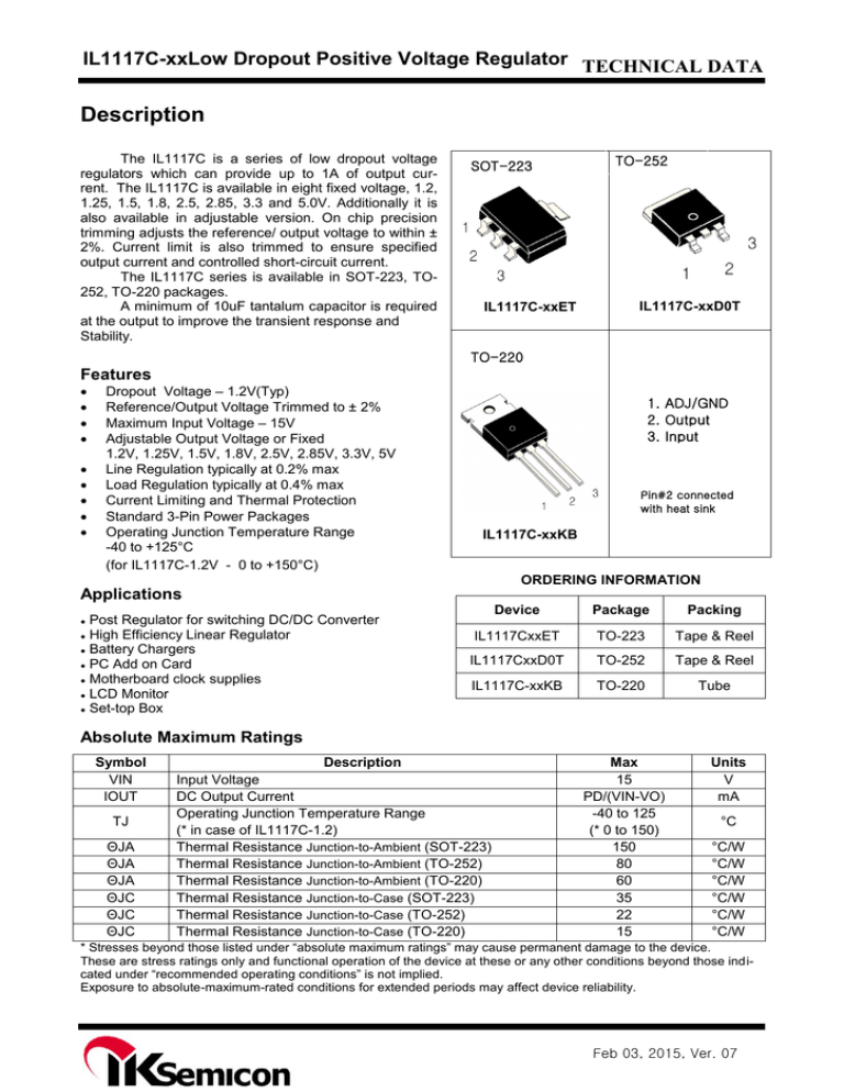
IL1117C-xxLow Dropout Positive Voltage Regulator TECHNICAL DATA Description The IL1117C is a series of low dropout voltage regulators which can provide up to 1A of output current. The IL1117C is available in eight fixed voltage, 1.2, 1.25, 1.5, 1.8, 2.5, 2.85, 3.3 and 5.0V. Additionally it is also available in adjustable version. On chip precision trimming adjusts the reference/ output voltage to within ± 2%. Current limit is also trimmed to ensure specified output current and controlled short-circuit current. The IL1117C series is available in SOT-223, TO252, TO-220 packages. A minimum of 10uF tantalum capacitor is required at the output to improve the transient response and Stability. SOT-223 IL1117C-xxET TO-252 IL1117C-xxD0T TO-220 Features Dropout Voltage – 1.2V(Typ) Reference/Output Voltage Trimmed to ± 2% Maximum Input Voltage – 15V Adjustable Output Voltage or Fixed 1.2V, 1.25V, 1.5V, 1.8V, 2.5V, 2.85V, 3.3V, 5V Line Regulation typically at 0.2% max Load Regulation typically at 0.4% max Current Limiting and Thermal Protection Standard 3-Pin Power Packages Operating Junction Temperature Range -40 to +125°C (for IL1117C-1.2V - 0 to +150°C) 1. ADJ/GND 2. Output 3. Input Pin#2 connected with heat sink IL1117C-xxKB ORDERING INFORMATION Applications Post Regulator for switching DC/DC Converter ● High Efficiency Linear Regulator ● Battery Chargers ● PC Add on Card ● Motherboard clock supplies ● LCD Monitor ● Set-top Box Device Package Packing IL1117CxxET TO-223 Tape & Reel IL1117CxxD0T TO-252 Tape & Reel IL1117C-xxKB TO-220 Tube ● Absolute Maximum Ratings Symbol VIN IOUT TJ ΘJA ΘJA ΘJA ΘJC ΘJC ΘJC Description Input Voltage DC Output Current Operating Junction Temperature Range (* in case of IL1117C-1.2) Thermal Resistance Junction-to-Ambient (SOT-223) Thermal Resistance Junction-to-Ambient (TO-252) Thermal Resistance Junction-to-Ambient (TO-220) Thermal Resistance Junction-to-Case (SOT-223) Thermal Resistance Junction-to-Case (TO-252) Thermal Resistance Junction-to-Case (TO-220) Max 15 PD/(VIN-VO) -40 to 125 (* 0 to 150) 150 80 60 35 22 15 Units V mA °C °C/W °C/W °C/W °C/W °C/W °C/W * Stresses beyond those listed under “absolute maximum ratings” may cause permanent damage to the device. These are stress ratings only and functional operation of the device at these or any other conditions beyond those indicated under “recommended operating conditions” is not implied. Exposure to absolute-maximum-rated conditions for extended periods may affect device reliability. Feb 03, 2015, Ver. 07 IL1117C-XX Electrical Characteristics Tj = -40°C to +125°C ( for IL1117C-1.2 Tj = 0 to +150°C) unless otherwise specified PARAMETER OUTPUT VOLTAGE IL1117C-1.2 IL1117C-1.25 (Adjustable) IL1117C-1.5 IL1117C-1.8 IL1117C-2.5 IL1117C-2.85 IL1117C-3.3 IL1117C-5.0 LINE REGULATION IL1117C-1.2 IL1117C-1.25 (Adjustable) IL1117C-1.5 IL1117C-1.8 IL1117C-2.5 IL1117C-2.85 IL1117C-3.3 IL1117C-5.0 LOAD REGULATION IL1117C-1.2 IL1117C-1.25 (Adjustable) IL1117C-1.5 IL1117C-1.8 IL1117C-2.5 IL1117C-2.85 IL1117C-3.3 IL1117C-5.0 CONDITIONS MIN TYP MAX UNIT 1.176 1.225 1.470 1.764 2.450 2.790 3.240 4.900 1.200 1.250 1.500 1.800 2.500 2.850 3.300 5.000 1.224 1.280 1.530 1.836 2.550 2.910 3.360 5.100 V Io =10mA, Vin = 2.7 to 12.0V Io =10mA, Vin = 2.8 to 12.0V Io =10mA, Vin = 3.0 to 12.0V Io =10mA, Vin = 3.3 to 12.0V Io =10mA, Vin = 4.0 to 12.0V Io =10mA, Vin = 4.4 to 12.0V Io =10mA, Vin = 4.8 to 12.0V Io =10mA, Vin = 6.5 to 12.0V 2.0 0.1 2.0 2.0 2.0 2.0 3.0 4.0 7.0 0.2 7.0 7.0 7.0 7.0 7.0 10.0 mV % mV mV mV mV mV mV Io = 10mA to 1.0A, Vin Io = 10mA to 1.0A, Vin Io = 10mA to 1.0A, Vin Io = 10mA to 1.0A, Vin Io = 10mA to 1.0A, Vin Io = 10mA to 1.0A, Vin Io = 10mA to 1.0A, Vin Io = 10mA to 1.0A, Vin 3.0 0.2 3.0 3.0 3.0 3.0 4.0 5.0 10.0 0.4 10.0 10.0 10.0 10.0 12.0 15.0 mV % mV mV mV mV mV mV Io = 10mA to 1.0A, Vin = 2.7 to 12.0V Io = 10mA to 1.0A, Vin = 2.8 to 12.0V Io = 10mA to 1.0A, Vin = 3.0 to 12.0V Io = 10mA to 1.0A, Vin = 3.3 to 12.0V Io = 10mA to 1.0A, Vin = 4.0 to 12.0V Io = 10mA to 1.0A, Vin = 4.4 to 12.0V Io = 10mA to 1.0A, Vin = 4.8 to 12.0V Io = 10mA to 1.0A, Vin = 6.5 to 12.0V = 3.2V = 3.3V = 3.5V = 3.8V = 4.5V = 4.85V = 5.3V = 7.0V DROPOUT VOLTAGE (2) All Models Io =1A (Tj = 25°C) 1.20 1.30 1.20 1.55 CURRENT LIMIT Io =1A (Tj = -40°C to +125°C) Vin - Vo = 5V (Tj = 25°C) Minimum Load Current Adjustable Models Vin = 13.75V QUIESCENT CURRENT Vin - Vo = 1.5V Adjust Pin Current vs Load Current, IL1117C TEMPERATURE DRIFT RMS Output Noise Ripple Rejection Ratio 1000 V mA 5 mA 5.2 10 mA Io = 10mA, Vin - Vo = 1.4 to 10V Io = 10mA to 1A, Vin - Vo = 1.4 to 10V Tj = -40°C to +125°C 50 0.5 0.5 120 5 uA uA % Bandwidth of 10Hz to 10kHz at 25°C 120Hz input Ripple(Cadj for ADJ) = 25uF Vin -Vo = 5V, Io = 1.0A Tj = -40°C to +125°C 0.003 %Vo 72 dB 60 NOTES: (1) IL1117C-x adjustable versions require a minimum load current for ±3% regulation. (2) Dropout voltage is the input voltage minus output voltage that produces a 1% decrease in output voltage. Feb 03, 2015 Ver. 07 IL1117C-XX Block Diagram Application Information IL1117C FIGURE 1. Fixed-Voltage Model —Basic Connections. IL1117C (Adj) FIGURE 2. Adjustable-Voltage Model --Basic Connections. Vo=Vref(1+R2/R1) + Iadj*R2 Feb 03, 2015 Ver. 07 IL1117C-XX Typical Perfomance Characteristics Feb 03, 2015 Ver. 07 IL1117C-XX Typical Perfomance Characteristics (continue) Figure 3. Feb 03, 2015 Ver. 07 IL1117C-XX Application Information Output voltage adjustment Like most regulators, the IL1117C regulates the output by comparing the output voltage to an internally generated reference voltage. On the adjustable version as shown in Fig.4, the VREF is available externally as 1.25V between VOUT and ADJ. The voltage ratio formed by R1 and R2 should be set to conduct 10mA (minumum output load). The output voltage is given by the following equation: Vo=Vref(1+R2/R1)+Iadj*R2 On fixed versions of IL1117C, the voltage divider is provided internal- ly. Figure 4. Basic Adjustable Regulator Input Bypass Capacitor An input capacitor is recommended. A 10μF tantalum on the input is a suitable input bypassing for almost all applications. Adjust Terminal Bypass Capacitor The adjust terminal can be bypassed to ground with a bypass capacitor (CADJ) to improve ripple rejection. This bypass capacitor prevents ripple from being amplified as the output voltage is increased. At any ripple frequency, the impedance of the CADJ should be less than R1 to prevent the ripple from being amplified: The R1 is the resistor between the output and the adjust pin. Its value is normally in the range of 100- 200Ω. For example, with R1 = 124Ωand fRIPPLE = 120Hz, the CADJ should be 11μF. Output Capacitor IL1117C requires a capacitor from VOUT to GND to provide compensation feedback to the internal gain stage. This is to ensure stability at the output terminal. Typically, a 10μF tantalum or 50μF aluminum electrolytic is sufficient. Note: The ESR is typically 1.0 Ω. The output capacitor does not have a theoretical upper limit and increasing its value will increase stability. COUT = 100μF or more is typical for high current regulator design. Load Regulation When the adjustable regulator is used (Fig.5), the best load regulation is accomplished when the top of the resistor divider (R1) is connected directly to the output pin of the IL1117C. When so connected, RP is not multiplied by the divider ratio. For Fixed output version, the top of R1 is internally connected to the output and ground pins can be connected to low side of the load. Feb 03, 2015 Ver. 07 IL1117C-XX Figure 5. Best Load Regulation Using Adjustable Output Regulator Thermal Protection IL1117C has thermal protection which limits junction temperature to 150C. However, device functionality is only guaranteed to a maximum junction temperature of +125C. The power dissipation and junction temperature for IL1117C in DPAK package are given by Note: TJUNCTION must not exceed 125C Current Limit Protection IL1117C is protected against overload conditions. Current protection is triggered at typically 1.6A. Thermal Consideration The IL1117C series contain thermal limiting circuitry designed to protect itself from over-temperature conditions. Even for normal load conditions, maximum junction temperature ratings must not be exceeded. As mention in thermal protection section, we need to consider all sources of thermal resistance between junction and ambient. It includes junction-tocase, case-to-heat-sink interface, and heat sink thermal resistance itself. Junction-to-case thermal resistance is specified from the IC junction to the bottom of the case directly below the die. Proper mounting is required to ensure the best possible thermal flow from this area of the package to the heat sink. The case of all devices in this series is electrically connected to the output. Therefore, if the case of the device must be electrically isolated, a thermally conductive spacer is recommended. Feb 03, 2015 Ver. 07 IL1117C-XX Symbol Dimension in Millimeters Dimension in inches Min Max Min Max A 1.520 1.800 0.060 0.071 A1 0.000 0.100 0.000 0.004 A2 1.600 1.700 0.063 0.067 b 0.680 0.780 0.027 0.031 c 0.230 0.280 0.009 0.011 D 6.400 6.500 0.252 0.256 D1 2.950 3.070 0.116 0.121 E 3.400 3.600 0.134 0.142 E1 6.800 7.200 0.268 0.283 e 2.300 (BSC) 0.091 (BSC) e1 4.6 (BSC) 1.811 (BSC) L 0.450 0.650 0.018 0.026 Θ 0ㅇ 10 ㅇ 0ㅇ 10 ㅇ Feb 03, 2015 Ver. 07 IL1117C-XX Feb 03, 2015 Ver. 07 IL1117C-XX Feb 03, 2015 Ver. 07

