Supertex inc.
HV9973
Isolated, Constant Current
LED Driver
Features
General Description
►► Programmable true constant current operation
►► ±3% LED current accuracy
►► Adaptive to external component tolerances and
parasitics
►► Primary-side current sensing
►► Output open circuit protection
►► Output short circuit protection
►► Input under voltage lockout
►► PWM dimming / enable
►► 280-400VDC input
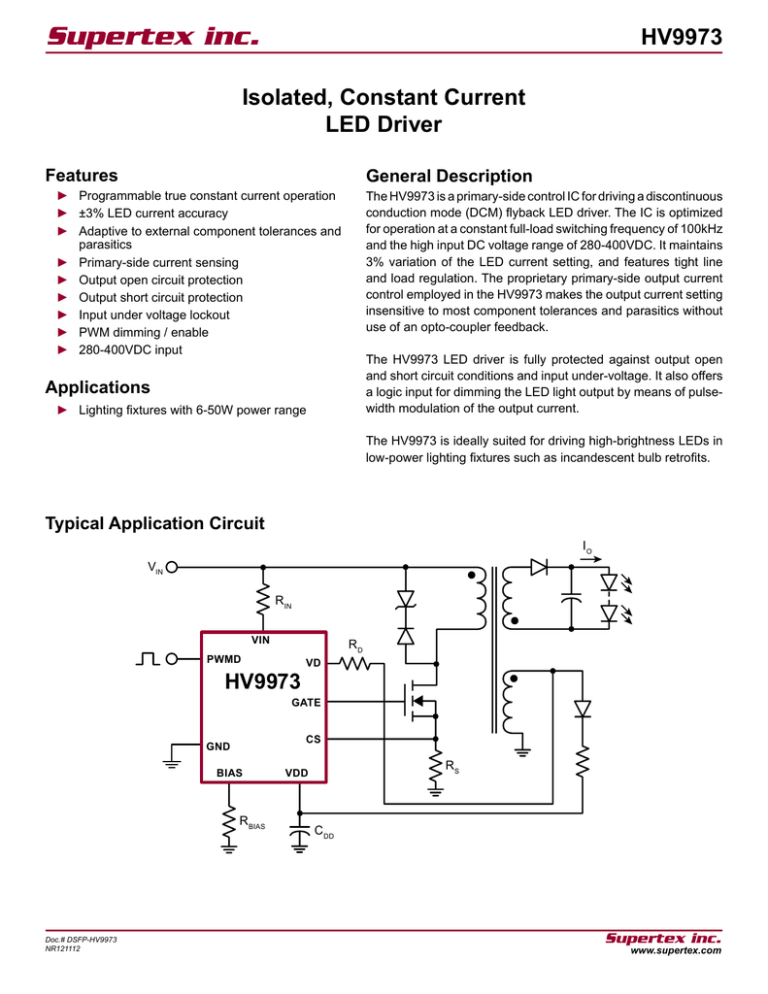
The HV9973 is a primary-side control IC for driving a discontinuous
conduction mode (DCM) flyback LED driver. The IC is optimized
for operation at a constant full-load switching frequency of 100kHz
and the high input DC voltage range of 280-400VDC. It maintains
3% variation of the LED current setting, and features tight line
and load regulation. The proprietary primary-side output current
control employed in the HV9973 makes the output current setting
insensitive to most component tolerances and parasitics without
use of an opto-coupler feedback.
The HV9973 LED driver is fully protected against output open
and short circuit conditions and input under-voltage. It also offers
a logic input for dimming the LED light output by means of pulsewidth modulation of the output current.
Applications
►► Lighting fixtures with 6-50W power range
The HV9973 is ideally suited for driving high-brightness LEDs in
low-power lighting fixtures such as incandescent bulb retrofits.
Typical Application Circuit
IO
VIN
R IN
VIN
RD
PWMD
HV9973
VD
GATE
CS
GND
BIAS
R BIAS
Doc.# DSFP-HV9973
NR121112
RS
VDD
C DD
Supertex inc.
www.supertex.com
HV9973
Pin Configuration
Ordering Information
Part Number
Package Option
Packing
HV9973LG-G
8-Lead SOIC
2500/Reel
VIN 1
8 GND
VD 2
-G indicates package is RoHS compliant (‘Green’)
7 PWMD
VDD 3
6 BIAS
CS 4
5 GATE
8-Lead SOIC
Product Marking
Absolute Maximum Ratings*
Parameter
VIN, VD, BIAS current
-0.3V to VDD(SHUNT)
VDD current
10mA
GATE voltage
-0.3V to VDD +0.3V
CS, PWMD voltage
-0.3V to 6.0V
Continuous power dissipation
630mW
Junction temperature
+125°C
(TA = +25°C) (derate 6.3mW/°C above +25°C)
Storage temperature range
H9973
LLLL
±5.0mA
VDD voltage
Y = Last Digit of Year Sealed
WW = Week Sealed
L = Lot Number
= “Green” Packaging
YWW
Value
Package may or may not include the following marks: Si or
8-Lead SOIC
Typical Thermal Resistance
Package
θja
8-Lead SOIC
101OC/W
-65°C to +150°C
* All voltages referenced to GND pin.
Stresses beyond those listed under “Absolute Maximum Ratings” may cause
permanent damage to the device. These are stress ratings only, and functional
operation of the device at these or any other conditions beyond those indicated in
the operational sections of the specifications is not implied. Exposure to absolute
maximum rating conditions for extended periods may affect device reliability.
Electrical Characteristics
(Specifications are at TA = 25°C, VDD = 10V, IIN = 200µA, CGATE = 750pF, BIAS open, unless otherwise noted).
Sym
Description
Min
Typ
Max
Units
Conditions
Power Supply (VDD)
VDD(SHUNT)
Shunt voltage
*
10.50
11.00
11.50
V
---
VDD(START)
Start voltage
*
9.95
10.50
11.45
V
VDD rising
VDD(STOP)
Under voltage threshold
*
6.65
7.00
7.70
V
VDD falling
IDDQ
Supply standby current
-
-
-
1.0
mA
Gate open
Start-up current
*
-
-
65
μA
VDD = 10V
IDDQ(START)
Notes:
* Specifications which apply over the full operating ambient temperature range of -40OC < TA < +125OC.
† Parameters guaranteed by design
Doc.# DSFP-HV9973
NR121112
2
Supertex inc.
www.supertex.com
HV9973
Electrical Characteristics
Sym
Description
Min
Typ
Max
Units
Conditions
Feed Forward Inputs (VD, VIN) and Oscillator
IIN
Operating current range
*
0
-
1000
μA
---
ID
Operating current range
*
0
-
1000
μA
---
VIN Input charge swing
*†
-
-
395
pF
IIN = 200μA, ID = 0
Oscillator coefficient
*
†
0.555
0.572
0.589
-
---
VD voltage
*
2.406
2.440
2.474
mV
---
Start-up frequency
-
-
10
-
kHz
---
Effective integrator capacitance
ratio VIN to VD
†
-
0.5
-
-
---
*
1198
1220
1242
mV
---
ΔQIN(MAX)
KOsc
VD
FS(START)
KC
Bias Current Generator (BIAS)
VBIAS
Output voltage
GATE Output
TRISE
GATE output rise time
-
-
40
75
ns
---
TFALL
GATE output fall time
-
-
20
40
ns
---
Current Sense Comparator
VCS(TH)
CS trip threshold
*
1198
1220
1242
mV
---
TDELAY
Propagation delay CS to GATE
*
-
-
100
ns
(VCS - VCS(TH)) = 20mV
TBLANK
Leading edge blanking delay
*
200
300
400
ns
---
VIN undervoltage threshold current
-
112
-
128
μA
VIN falling
VDD undervoltage lockout hysteresis
-
-
20
-
μA
VIN rising
-
66.5
-
73.5
μA
---
VIN Under Voltage Comparator
IIN(UVLO)
ΔIIN(UVLO)
Open Circuit Protection
ID(OV)
Output open circuit threshold
PWM Dimming
VPWMD,HI
PWMD input high voltage
*
2.0
-
-
V
---
VPWMD,LO
PWMD input low voltage
*
-
-
0.8
V
---
Effective Current Sense Reference Voltage
VEFF
ΔVEFF/VEFF
Effective reference voltage
-
333
-
361
mV
IIN, ID regulation of VEFF
†
-
3.0
-
%
IIN = 162.5μA, ID = 120μA,
See Note 1.
125μA ≤IIN ≤ 185μA,
40μA ≤ID ≤ 120μA
Notes:
* specifications which apply over the full operating ambient temperature range of -40OC < TA < +125OC.
† Parameters guaranteed by design.
1. Effective output current VEFF = 0.5 • VCS • KOsc. Trimmed to the product of VCS • KOsc.
Doc.# DSFP-HV9973
NR121112
3
Supertex inc.
www.supertex.com
HV9973
Functional Block Diagram
VD
VDD
VIN
UVLO
iD
iIN
11V
Shunt
Reg.
Start-Up
Oscillator
2.44V
Current
Mirror
PWMD
Shutdown
S&H
GATE
iIN
iIN
iD - iBIAS
VIN
UVLO
<iD - iBIAS>
UV Power-On Reset
(sampled)
Oscillator
&
Parasitics
Compensator
UV
iUV
Q R
+
-
S
L/E
Blanking
1.22V
CS
CLK
OVP
Shutdown
BIAS
Q S
Power-On Reset
<iD - iBIAS>
(sampled)
R
iOVP
1.22V
GND
iBIAS
BIAS
Doc.# DSFP-HV9973
NR121112
4
Supertex inc.
www.supertex.com
HV9973
Functional Description
Power Topology and Control Method
The HV9973 regulates the constant output current of a discontinuous conduction mode (DCM) flyback converter. Although it can be used in other applications, it is optimized for
operating from a high DC line input voltage of 280-400VDC.
The HV9973 is a fully integrated peak-current PWM controller IC. It does not require an optocoupler feedback, and includes protection from output open-circuit, short-circuit, and
input under-voltage conditions. A proprietary control scheme
permits accurate primary-side control of output current, insensitive to most circuit parasitics, external component tolerances and output voltage variation.
where:
VOR = n • (VO + VF )
IO =
IPK • n • KOsc
2
Proper selection of maximum switching frequency FS(MAX) at
full load, in combination with maximum VOR(MAX) is critical for
proper operation of the HV9973. The oscillator circuit ramp
may saturate when the maximum charge swing ΔQIN(MAX) =
400pC is exceeded at VIN. Therefore, the circuit components
should be selected such that:
(1)
2 • RS
=
n • VEFF
RS
(3)
The effective reference voltage VEFF = 347mV. Hence, the
desired LED current is programmed by merely selecting the
current sense resistor as:
RS =
n • VEFF
IO
≤ ΔQIN(MAX)
(7)
VOR(MAX) • KOsc(MAX) Lm(MAX) VCS(TH)MAX RS(MAX)
•
•
•
≤ ΔQIN(MAX)
FS(MAX) • RIN(MIN)
Lm(MIN) VCS(TH)MIN RS(MIN)
(9)
(4)
The equation (9) gives the condition for selecting proper
ratio of VOR(max)/FS(MAX), which guarantees ΔQIN ≤ QIN(MAX).
Selection of the resistor RIN is dictated by the desired input
under-voltage (UV). The recommended selection of RIN =
2.0MΩ produces a UV shutdown at VIN < 240VDC. As an example, we can assume the tolerances of Lm and RS as ±10%
and ±1% correspondingly. We shall also limit the switching
frequency under FS(MAX) = 130KHz. With these assumption,
the equation (9) gives VOR(MAX) ≤ 134.1V. Apparently, there
Note that the output current of the HV9973 LED driver is
independent of the input and output voltage, the switching
frequency or the transformer inductance.
The switching frequency at a given output voltage VO can be
estimated as:
n • (VO + VF ) • KOsc VOR • KOsc
=
(5)
FS =
Lm • IPK
Lm • IPK
Doc.# DSFP-HV9973
NR121112
RIN
Therefore, the charge swing ΔQIN varies only as a function
of external component tolerances and circuit parasitic, and it
is the same for all VIN and VO operating conditions. Combining equations (5), (7) and (8), and taking into consideration
tolerances for Lm, RS and VCS(TH), we get the following design
criterion:
Combining (1) and (2), we can write the output current as:
VCS(TH) • n • KOsc
VIN • TON
The transformer magnetic flux equals the volt-seconds at
the transformer winding in the DCM flyback converter:
VIN • TON ≈ LM • IPK (8)
In (2), VCS(TH) is the reference voltage of the current sense
comparator at CS, and RS is the current sense resistance.
IO =
ΔQIN =
Note, that the HV9973 is protected against incorrect oscillator setup. When saturation of the oscillator ramp occurs,
the HV9973 shuts off and attempts to go through a start-up
cycle again.
Where KOsc = 0.572 is an oscillator coefficient, n is flyback
transformer turns ratio of primary to secondary winding, and
where IPK is peak primary winding current given by:
VCS(TH)
IPK =
(2)
RS
(6)
In the equation (5), Lm is magnetizing inductance of the
transformer primary winding, and VF is the forward voltage
drop at the output rectifier diode. (Note that the switching
frequency is not a function of the internal timing components
of the HV9973 or the absolute value of RIN and RD).
Output current of an HV9973 flyback converter can be expressed as:
5
Supertex inc.
www.supertex.com
HV9973
the voltage at VDD falls below VDD(UV) = 7.0V. Under steadystate operation, the IC is powered by an auxiliary bootstrap
winding through a ballast resistor RDD. The primary-to-auxiliary winding turn ratio nAUX and the value of RDD should be
selected carefully to ensure operation throughout the input
and output voltage range with minimum power dissipation
in RDD. Note that the polarity of the auxiliary winding is opposite of the polarity of the secondary winding, such that the
auxiliary winding voltage is positive during the on time. The
following formulas are providing optimal values for nAUX and
RDD, given the output voltage range VO(MIN), VO(MAX) and the
input voltage range VIN(MIN), VIN(MAX):
is also limitation on V(OR)MAX related to open circuit protection:
V(OR)MAX < RIN(MIN) • ID(OV)MIN (9A). In our case V(OR)MAX < 120.2V
and the least of two values should be used. With some margin
we should choose V(OR)MAX = 120V.
The above example takes full advantage of the available VIN
input dynamic range, and, therefore, achieves the most accurate control over the LED current. For this reason, we will
use VOR(MAX) = 120V and FS(MAX) = 130KHz in the following
equations, as our recommended design inputs. Given, the
primary-to-secondary turn ratio is determined simply as:
VOR(MAX)
120V
n=
=
(10)
(VO(MAX) + VF ) (VO(MAX) + VF )
VIN(MIN) • VIN(MAX)
(14)
nAUX =
2 • VDD(UV) • VIN(MAX) – VIN(MIN) • VDD(REG)
(
2
where WDD is power dissipation in RDD, and IDDQ is the quiescent current of the HV9973.
Start-Up
Upon applying the input AC power, the input current of VIN
is diverted into the hold-up capacitor connected at VDD.
The HV9973 consumes less than 60µA in this mode, and
its GATE output is off. When a threshold of VDD = 10.5V is
reached at VDD, VIN is disconnected from VDD, and the
GATE output turns on. The GATE turns off upon reaching
VCS(TH) = 1.22V at CS. The frequency of the GATE pulses is
determined by the oscillator circuit or by the 10kHz start-up
clock, whichever frequency is higher.
(13)
The hold-up capacitor connected at VDD must store enough
energy to supply power to the HV9973 until adequate bootstrap power supply becomes available. The HV9973 stops
switching and makes another attempt to charge the hold-up
capacitor, if the voltage at VDD falls below 7.0V.
Here, LLK is primary winding leakage inductance, VZ is the
Zener clamp voltage. Hence, the Zener clamp voltage VZ
should be selected significantly higher than n•(VO(MAX) + VF).
VZ must also exceed the open-circuit protection threshold.
Although the resistor RIN serves a different purpose in operation, its value must be selected with care to ensure the
required 60µA start-up current at VIN(MIN).
The HV9973 is powered by an internal shunt regulator,
clamping VDD at VDD(REG) = 11V. The IC shuts down when
Doc.# DSFP-HV9973
NR121112
VIN(MAX)
– VDD(REG) • n • (VO(MAX) + VF ) • KOsc
nAUX
(16)
WDD =
RDD • VIN(MAX)
Due to presence of the leakage inductance LLK, a voltage
spike occurs at the primary winding of the transformer. Although the HV9973 eliminates the effect of the leakage
inductance on the LED current, the duration of this spike
should be minimized for best efficiency. The time tLK is the
leakage spike duration, determined by:
LLK • IPK
VZ – n • (VO(MAX) + VF )
VDD(REG)
(
(
Selection of the maximum magnetizing inductance in accordance with (11) guarantees DCM operation in the entire
working range of the input voltage with the proper selection
of the input under-voltage and output over-voltage thresholds. (See “Input Under-Voltage Protection” and “Output
Open and Short Circuit Protection” below.)
tLK =
–
• n • (VO(MIN) + VF ) • KOsc
VIN(MIN) VIN(MAX)
(15)
RDD =
(VO(MIN) + VF )
IDDQ + QGATE •
• FS(MAX)
(VO(MAX) + VF )
If we assume the primary inductance tolerance of ±10%, the
nominal value of Lm is determined simply as:
Lm(MAX)
Lm =
(12)
1.1
VDD(UV)
(
The maximum magnetizing inductance of the primary winding Lm(MAX) is obtained by combining the equations (2), (7)
and (8):
ΔQIN(MAX) • RIN(MIN) • RS(MIN)
(11)
Lm(MAX) =
VCS(TH)MAX
6
Supertex inc.
www.supertex.com
HV9973
Current Sense Comparator
The peak current comparator is using an external sense
resistor RS to compare the primary winding current to the
reference voltage VCS(TH) = 1.22V. The corresponding peak
current IPK is given by equation (2). When the current in the
primary winding exceeds IPK, the comparator resets the
PWM flip-flop circuit, and the output pulse is terminated.
The next cycle begins upon receiving a clock signal from an
internal oscillator circuit. A 300ns leading-edge blanking delay is applied to prevent false triggering of the current sense
comparator.
iIN =
VIN –1V
RIN
≈
VIN
RIN
RD =
(17)
Accordingly, the input current iD is derived by connecting a
resistor RD from the bootstrap winding to VD. However, since
nAUX >> 1 normally, the voltage VAUX is much higer in comparison to the voltage at the VD pin (VD = 2.44V). Hence, the
current iD through the resistor RD can be expressed as:
iD =
VD – VAUX
RD
iOS =
VD
RD
iBIAS =
RBIAS =
7
(20)
(22)
nAUX
(23)
LS(AUX)
(24)
LAUX
FS =
n • (VO + VF ) • KOsc • RS
Lm • VCS(TH)
(25)
VO(LIM) =
RD • nAUX
n
• 66.5µA – VF
(26)
Normal operation resumes when the adequate LED load is
connected.
Output short circuit protection is inherent to the HV9973
since the switching frequency is directly proportional to the
output voltage. Moreover, loss of output voltage is likely to
cause insufficient bootstrap power at VDD, resulting in a
“hiccup” operating mode and repetitive restart attempts.
(21)
The resulting current iOR = (iD - iOS) represents the instantaneous voltage across the transformer bootstrap winding:
Doc.# DSFP-HV9973
NR121112
RD
Output Open and Short Circuit Protection
The HV9973 provides a very reliable open circuit protection.
If the sampled current iOR exceeds the 140µA threshold, the
HV9973 is forced to go through a power-up cycle again. The
corresponding output voltage threshold can be calculated
as:
In (20), VBIAS = VD/2 is the voltage at the BIAS pin. Combining the equations (19) and (20) gives formula for calculating
RBIAS simply as:
RD
VAUX
RIN • KC • k
k= 1–
(19)
VBIAS
3.5 • iOS
3.5 • RBIAS
=–
With proper selection of the resistor RD in accordance with
(23), the oscillator circuit then generates switching frequency:
(18)
The HV9973 cancels out this offset internally by subtracting
a current of the same magnitude as iOS. This correction current is programmed by connecting a resistor at the BIAS pin
in accordance with:
VBIAS
Here, LAUX is the bootstrap winding inductance. Since the
value of the k is normally very close to 1, then k = 1 could be
used as a first approximation.
From this equation, the current iD is not directly proportional
to VAUX. The offset current is given by the following equation:
RD
–
In (23), k is the coupling coefficient between the primary
and the bootstrap windings. The coupling coefficient can be
determined by measuring the leakage inductance LS(AUX) of
the auxiliary winding with respect to the primary winding and
calculating it in accordance with the equation:
VD – VAUX
Sampled during the conduction time of the transformer secondary winding, this current represents the reflected output
voltage (VO + VF), where VF is the voltage drop across the
output rectified diode. The value of RD should scale with RIN
in accordance with:
Oscillator Circuit
Upon the end of the start-up cycle, the input current of VIN is
reverted to a current mirror circuit for generating the current
iIN in accordance with the following equation:
iOR =
7
Supertex inc.
www.supertex.com
HV9973
Input Under-Voltage Protection
The GATE output of the HV9973 becomes inhibited when
the input current at VIN falls below 120µA. The GATE output
is enabled again when the VIN current exceeds 140µA. The
corresponding input under-voltage thresholds can be calculated as:
VIN(STOP) = RIN • 120µA (27)
VIN(START) = RIN • 140µA than being wired to ground or across the primary winding.
Otherwise, the current from CSN may cause false tripping of
the CS comparator.
Power dissipation in RSN can be estimated by the following
formula:
WRSN = CSN • VIN(MAX)2 • FS(MAX) (31)
Layout Considerations
The signal inputs VIN and VD operate at relatively low input current ranging from hundreds down to tens of microamps. Therefore, proximity of the switching potential of the
MOSFET drain can cause a displacement current in VD and
VIN affecting the normal operation of the HV9973. Proper
HV9973 PCB layout should avoid direct proximity of the VD
and VIN inputs to the high-voltage switching potential.
(28)
R-C Snubber Design Considerations
Detection of tLK given by the equation (13) is crucial for proper operation of the HV9973. Upon the turn-off of the switching MOSFET, the voltage spike caused by the transformer
leakage inductance is followed by high-frequency oscillation. The oscillation occurs at the transformer windings with
the period equal to 2π√LLK • COSS , where COSS is the output capacitance of the MOSFET. This oscillation is damped
naturally by copper and core losses of the transformer, and
it subsides during conduction time of the secondary winding.
However, extra damping is usually required. Insufficiently
damped, the post-spike oscillation may adversely affect accuracy of the output current regulation as well as EMI performance of the LED driver.
The resistor RD should be placed as close as possible to the
VD input. Otherwise, a long VD trace can be susceptible to
noise coupling, or it can introduce parasitic capacitance with
respect to ground capable of distorting the VD input signal.
Design example
The following example illustrates LED driver design with
HV9973 for the following conditions:
Damping of the post-spike oscillation is achieved by connecting of a snubber network (RSN, CSN) across the switching MOSFET. Selection of the RSN and CSN values is based
on achieving sufficient damping while minimizing the power
losses in the snubber network. At the same time, the oscillation should not be over-damped, as this will prevent detection of tLK.
1. Input: VIN(MIN) = 240V, VIN(MAX) = 375V
2. Output: VO(MIN) = 6.0V, VO(MAX) = 18V, VF = 0.7V,
IO = 0.5A
3. Maximum switching frequency: FS(MAX) = 130kHz
4. VIN(STOP) = 240V
Design:
1. Using formula (27), calculate value of the resistor RIN:
We recommend the following choice of the snubber network
components:
CSN = COSS (29)
RIN =
RSN = 1.6
LLK
CSN
(30)
120µA
= 2.0MΩ
2. Using formula (9), calculate VOR(MAX):
ΔQIN(MAX) • FS(MAX) •RIN
VOR =
• 77.6% = 134.1V
KOsc(MAX)
Note that the output capacitance COSS is a nonlinear function
of the drain voltage. Most datasheets give the COSS value at
the drain voltage of VDS = 25V. Typically, the output capacitance characteristic as a function of VDS is provided in the
MOSFET datasheet as well. The equation (29) should use
the COSS value at VDS = (VIN(MIN) + n•VO(MIN)), or at the highest
VDS given in the plot, whichever voltage is lower.
Using formula (9A), calculate V(OR)MAX base on OV protection:
Also note that the R-C snubber network must be connected
between the drain and the source of the MOSFET, rather
Doc.# DSFP-HV9973
NR121112
VIN(STOP)
VOR = RIN(MIN) • ID(OV)MIN = 131.7V
Choose V(OR)MAX = 120V based on 8 - 10% margin from lower value.
8
Supertex inc.
www.supertex.com
HV9973
n=
VOR(MAX)
(VO(MAX) + VF )
=
115V
(VO(MAX) + VF )
9. Using formula (15), calculate value of the resistor RDD:
= 6.353
RDD =
n • VEFF
IO
VDD(REG)
VIN(MAX)
• n • (VO(MIN) + VF ) • KOsc(MAX)
= 62.0Ω
(VO(MIN) + VF )
(VO(MAX) + VF )
• FS(MAX)
( We have assumed QGATE = 15nC and VDD(MIN) = 8V to account for the forward voltage drop at the bootstrap winding
diode.)
= 4.47Ω
VIN(MIN)
–
IDDQ + QGATE •
4. Using formula (4), calculate value of the current sense
resistor:
RS =
(
VDD(UV)
(
3. Using formula (10), calculate primary-to-secondary turns
ratio of the flyback transformer:
5. Using formula (2), calculate value of the maximum peak 10. Using formula (18), calculate the maximum power discurrent:
sipation WDD in the resistor RDD:
VCS(TH)MAX VCS(TH)MAX
2
VIN(MAX)
IPK(MAX) =
=
= 0.277A –V
R
0.99
•
R
DD(REG) • n •(VO(MAX) + VF ) • KOsc(MAX)
S(MIN)
S
nAUX
WDD =
= 0.028W
RDD•VIN(MAX)
6. Using formula (11), calculate maximum value of the magnetizing inductance:
11. Using formula (30), calculate the resistor RSN. Assume
Lm(MAX) ΔQIN(MAX) • 0.99RIN • 0.99RS
Lm =
=
= 2.564µH C
= 33pF (IRFUC20, 600V, 1A MOSFET), LLK = 20μH:
OSS
110%
V
• 110%
(
(
CS(TH)MAX
CSN = 33pF 7. Using formula (14), calculate turns ratio primary-to-auxiliary winding of the flyback transformer:
nAUX =
VIN(MIN) •VIN(MAX)
2 •VDD(UV) • VIN(MAX) – VIN(MIN) •VDD(REG)
RSN = 1.6
= 6.72
RD =
nAUX
Doc.# DSFP-HV9973
NR121112
= 38.9kΩ
RD
RBIAS =
= 5.56kΩ
7
CSN
= 1.25k Ω
12. Using formula (30), calculate the maximum power dissipation WRSN in the resistor RSN:
8. Using formulas (21) and (23), calculate values of the resistors RD, RBIAS:
RIN
LLK
2
WRSN = CSN • VIN(MAX) • FS(MAX) = 0.6W
9
Supertex inc.
www.supertex.com
HV9973
Pin Description
Pin #
Function
1
VIN
This pin is the input voltage feed forward input. Connect a resistor from this pin to the input side of
the primary winding of the transformer to program the VIN current. The same resistor is also used
for start-up upon initial application of power.
2
VD
This pin is the auxiliary winding feedback input. Connect a resistor from this pin to the transformer
bootstrap winding.
3
VDD
This is a power supply pin for all internal circuits. It must be bypassed with a low ESR capacitor to
GND. The capacitor must be able to store sufficient energy for starting up the converter.
4
CS
5
GATE
This pin is the output gate driver for an external N-channel power MOSFET.
6
BIAS
This pin is used for generating a correction current to account for the 2.44V offset at VD. Connect a
resistor to ground to program.
7
PWMD
When this pin is pulled to GND, switching of the HV9973 is disabled. When the PWM pin is released,
or external TTL high level is applied to it, switching will resume.
8
GND
Doc.# DSFP-HV9973
NR121112
Description
This pin is for sensing peak output voltage at an external current sense resistor..
This pin is the common return for all the internal circuits.
10
Supertex inc.
www.supertex.com
HV9973
8-Lead SOIC (Narrow Body) Package Outline (LG)
4.90x3.90mm body, 1.75mm height (max), 1.27mm pitch
θ1
D
8
Note 1
(Index Area
D/2 x E1/2)
E1
E
Gauge
Plane
L2
L
1
θ
L1
Top View
View B
Note 1
Seating
Plane
View B
h
A
h
A A2
Seating
Plane
A1
e
b
Side View
View A-A
A
Note:
1. This chamfer feature is optional. A Pin 1 identifier must be located in the index area indicated. The Pin 1 identifier can be: a molded mark/identifier;
an embedded metal marker; or a printed indicator.
Symbol
Dimension
(mm)
A
A1
A2
b
MIN
1.35*
0.10
1.25
0.31
NOM
-
-
-
-
MAX
1.75
0.25
1.65*
0.51
D
E
E1
4.80* 5.80* 3.80*
4.90
6.00
3.90
5.00* 6.20* 4.00*
e
1.27
BSC
h
L
0.25
0.40
-
-
0.50
1.27
L1
1.04
REF
L2
0.25
BSC
θ
θ1
0O
5O
-
-
8O
15O
JEDEC Registration MS-012, Variation AA, Issue E, Sept. 2005.
* This dimension is not specified in the JEDEC drawing.
Drawings are not to scale.
Supertex Doc. #: DSPD-8SOLGTG, Version I041309.
(The package drawing(s) in this data sheet may not reflect the most current specifications. For the latest package outline
information go to http://www.supertex.com/packaging.html.)
Supertex inc. does not recommend the use of its products in life support applications, and will not knowingly sell them for use in such applications unless it receives
an adequate “product liability indemnification insurance agreement.” Supertex inc. does not assume responsibility for use of devices described, and limits its liability
to the replacement of the devices determined defective due to workmanship. No responsibility is assumed for possible omissions and inaccuracies. Circuitry and
specifications are subject to change without notice. For the latest product specifications refer to the Supertex inc. (website: http//www.supertex.com)
Supertex inc.
©2012 Supertex inc. All rights reserved. Unauthorized use or reproduction is prohibited.
Doc.# DSFP-HV9973
NR121112
11
1235 Bordeaux Drive, Sunnyvale, CA 94089
Tel: 408-222-8888
www.supertex.com
