Freescale Semiconductor
Technical Data
Heterojunction Bipolar Transistor
Technology (InGaP HBT)
MMG3001NT1
Broadband High Linearity Amplifier
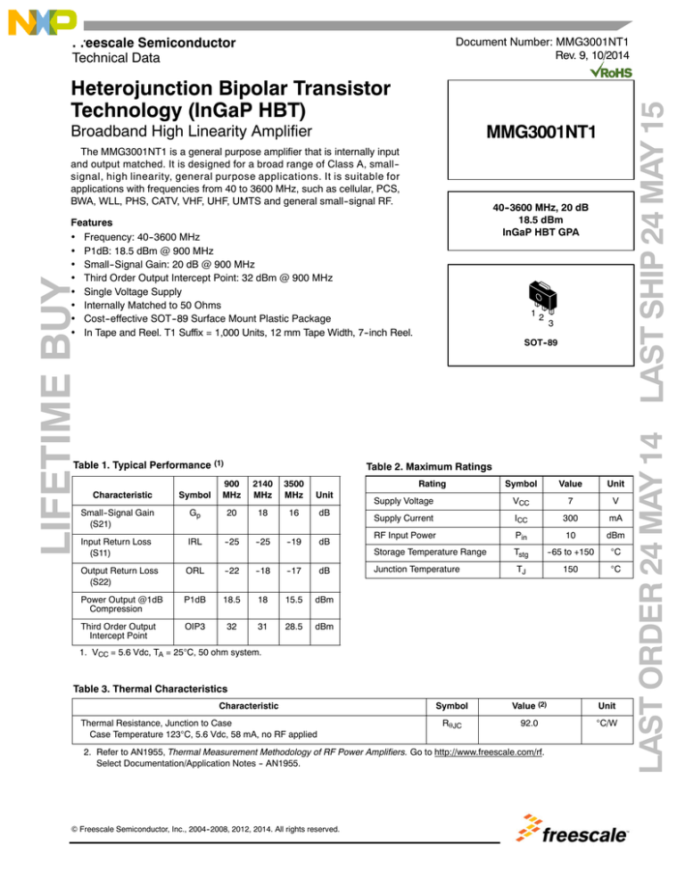
The MMG3001NT1 is a general purpose amplifier that is internally input
and output matched. It is designed for a broad range of Class A, small-signal, high linearity, general purpose applications. It is suitable for
applications with frequencies from 40 to 3600 MHz, such as cellular, PCS,
BWA, WLL, PHS, CATV, VHF, UHF, UMTS and general small--signal RF.
40--3600 MHz, 20 dB
18.5 dBm
InGaP HBT GPA
LIFETIME BUY
Features
Frequency: 40--3600 MHz
P1dB: 18.5 dBm @ 900 MHz
Small--Signal Gain: 20 dB @ 900 MHz
Third Order Output Intercept Point: 32 dBm @ 900 MHz
Single Voltage Supply
Internally Matched to 50 Ohms
Cost--effective SOT--89 Surface Mount Plastic Package
In Tape and Reel. T1 Suffix = 1,000 Units, 12 mm Tape Width, 7--inch Reel.
Table 1. Typical Performance (1)
3
SOT--89
Table 2. Maximum Ratings
Rating
Symbol
900
MHz
2140
MHz
3500
MHz
Unit
Small--Signal Gain
(S21)
Gp
20
18
16
dB
Input Return Loss
(S11)
IRL
--25
--25
--19
dB
Output Return Loss
(S22)
ORL
--22
--18
--17
dB
Power Output @1dB
Compression
P1dB
18.5
18
15.5
dBm
Third Order Output
Intercept Point
OIP3
32
31
28.5
dBm
Characteristic
12
Symbol
Value
Unit
Supply Voltage
VCC
7
V
Supply Current
ICC
300
mA
RF Input Power
Pin
10
dBm
Storage Temperature Range
Tstg
--65 to +150
C
Junction Temperature
TJ
150
C
1. VCC = 5.6 Vdc, TA = 25C, 50 ohm system.
Table 3. Thermal Characteristics
Characteristic
Thermal Resistance, Junction to Case
Case Temperature 123C, 5.6 Vdc, 58 mA, no RF applied
Symbol
Value (2)
Unit
RJC
92.0
C/W
2. Refer to AN1955, Thermal Measurement Methodology of RF Power Amplifiers. Go to http://www.freescale.com/rf.
Select Documentation/Application Notes -- AN1955.
Freescale Semiconductor, Inc., 2004--2008, 2012, 2014. All rights reserved.
RF Device Data
Freescale Semiconductor, Inc.
LAST ORDER 24 MAY 14 LAST SHIP 24 MAY 15
Document Number: MMG3001NT1
Rev. 9, 10/2014
MMG3001NT1
1
Characteristic
Symbol
Min
Typ
Max
Unit
Gp
18
20
—
dB
Input Return Loss (S11)
IRL
—
--25
—
dB
Output Return Loss (S22)
ORL
—
--22
—
dB
Power Output @ 1dB Compression
P1dB
—
18.5
—
dBm
Third Order Output Intercept Point
OIP3
—
32
—
dBm
Noise Figure
NF
—
4.1
—
dB
Supply Current
ICC
40
58
75
mA
Supply Voltage
VCC
—
5.6
—
V
Small--Signal Gain (S21)
LIFETIME BUY
Table 5. Functional Pin Description
2
Pin
Number
Pin Function
1
RFin
2
Ground
3
RFout/DC Supply
1
2
3
Figure 1. Functional Diagram
Table 6. ESD Protection Characteristics
Test Conditions/Test Methodology
Class
Human Body Model (per JESD 22--A114)
0
Machine Model (per EIA/JESD 22--A115)
A
Charge Device Model (per JESD 22--C101)
IV
Table 7. Moisture Sensitivity Level
Test Methodology
Per JESD 22--A113, IPC/JEDEC J--STD--020
Rating
Package Peak Temperature
Unit
1
260
C
LAST ORDER 24 MAY 14 LAST SHIP 24 MAY 15
Table 4. Electrical Characteristics (VCC = 5.6 Vdc, 900 MHz, TA = 25C, 50 ohm system, in Freescale Application Circuit)
MMG3001NT1
2
RF Device Data
Freescale Semiconductor, Inc.
50 OHM TYPICAL CHARACTERISTICS
TC = 85C
25C
--10
20
--40C
15
S22
--20
S11
--30
VCC = 5.6 Vdc
VCC = 5.6 Vdc
10
--40
1
2
3
1
2
4
3
f, FREQUENCY (GHz)
Figure 2. Small--Signal Gain (S21) versus
Frequency
Figure 3. Input/Output Return Loss versus
Frequency
23
21
900 MHz
19
1960 MHz
17
2140 MHz
P1dB, 1 dB COMPRESSION POINT (dBm)
21
2600 MHz
3500 MHz
15
13
11
VCC = 5.6 Vdc
9
12
10
14
16
19
18
17
16
15
0.5
20
18
VCC = 5.6 Vdc
1
1.5
2
2.5
3
Pout, OUTPUT POWER (dBm)
f, FREQUENCY (GHz)
Figure 4. Small--Signal Gain versus Output
Power
Figure 5. P1dB versus Frequency
80
60
40
20
0
4.9
20
14
100
ICC, COLLECTOR CURRENT (mA)
0
4
f, FREQUENCY (GHz)
5
5.1
5.2
5.3
5.4
5.5
5.6
VCC, COLLECTOR VOLTAGE (V)
Figure 6. Collector Current versus Collector
Voltage
5.7
OIP3, THIRD ORDER OUTPUT INTERCEPT POINT (dBm)
Gp, SMALL--SIGNAL GAIN (dB)
LIFETIME BUY
0
3.5
33
30
27
24
21
VCC = 5.6 Vdc
100 kHz Tone Spacing
18
0
1
2
3
f, FREQUENCY (GHz)
Figure 7. Third Order Output Intercept Point
versus Frequency
LAST ORDER 24 MAY 14 LAST SHIP 24 MAY 15
0
S11, S22 (dB)
Gp, SMALL--SIGNAL GAIN (dB)
25
4
MMG3001NT1
RF Device Data
Freescale Semiconductor, Inc.
3
30
27
24
f = 900 MHz
100 kHz Tone Spacing
21
5.5
5.55
5.6
5.65
5.7
VCC, COLLECTOR VOLTAGE (V)
36
VCC = 5.6 Vdc
f = 900 MHz
100 kHz Tone Spacing
8 Vdc Supply with 43 Ω Dropping Resistor
35
34
33
32
31
30
--40
--20
20
40
60
80
100
T, TEMPERATURE (_C)
Figure 9. Third Order Output Intercept Point
versus Case Temperature
Figure 8. Third Order Output Intercept Point
versus Collector Voltage
105
--30
--40
MTTF (YEARS)
IMD, THIRD ORDER
INTERMODULATION DISTORTION (dBc)
0
--50
--60
104
VCC = 5.6 Vdc
f = 900 MHz
100 kHz Tone Spacing
--70
103
--80
0
3
6
9
12
120
18
15
125
Pout, OUTPUT POWER (dBm)
4
2
VCC = 5.6 Vdc
0
1
1.5
2
2.5
3
140
145
150
NOTE: The MTTF is calculated with VCC = 5.6 Vdc, ICC = 58 mA
3.5
4
Figure 11. MTTF versus Junction Temperature
ACPR, ADJACENT CHANNEL POWER RATIO (dBc)
6
0.5
135
TJ, JUNCTION TEMPERATURE (C)
Figure 10. Third Order Intermodulation Distortion
versus Output Power
0
130
--20
VCC = 5.6 Vdc, f = 2140 MHz
Single--Carrier W--CDMA, 3.84 MHz Channel Bandwidth
Input Signal PAR = 8.5 dB @ 0.01% Probability (CCDF)
--30
--40
--50
--60
--70
0
2
4
6
8
10
12
f, FREQUENCY (GHz)
Pout, OUTPUT POWER (dBm)
Figure 12. Noise Figure versus Frequency
Figure 13. Single--Carrier W--CDMA Adjacent
Channel Power Ratio versus Output Power
LAST ORDER 24 MAY 14 LAST SHIP 24 MAY 15
33
8
NF, NOISE FIGURE (dB)
OIP3, THIRD ORDER OUTPUT INTERCEPT POINT (dBm)
36
LIFETIME BUY
OIP3, THIRD ORDER OUTPUT INTERCEPT POINT (dBm)
50 OHM TYPICAL CHARACTERISTICS
14
MMG3001NT1
4
RF Device Data
Freescale Semiconductor, Inc.
50 OHM APPLICATION CIRCUIT: 40--800 MHz
R1
C3
C4
C5
L1
RF
INPUT
Z1
DUT
Z2
S21, S11, S22 (dB)
LIFETIME BUY
C1
Z1, Z5
Z2
Z3
Z3
Z4
RF
OUTPUT
Z5
C2
VCC
0.347 x 0.058 Microstrip
0.575 x 0.058 Microstrip
0.172 x 0.058 Microstrip
Z4
PCB
0.403 x 0.058 Microstrip
Getek Grade ML200C, 0.031, r = 4.1
Figure 14. 50 Ohm Test Circuit Schematic
30
S21
20
R1
10
0
L1
--10
C5
C4
C3
C2
C1
S22
--20
--30
0
200
MMG30XX
Rev 2
VCC = 5.6 Vdc
S11
--40
400
600
800
f, FREQUENCY (MHz)
Figure 16. 50 Ohm Test Circuit Component Layout
Figure 15. S21, S11 and S22 versus Frequency
Table 8. 50 Ohm Test Circuit Component Designations and Values
Part
Description
Part Number
Manufacturer
C1, C2, C3
0.01 F Chip Capacitors
C0603C103J5RAC
Kemet
C4
1000 pF Chip Capacitor
C0603C102J5RAC
Kemet
C5
47 pF Chip Capacitor
C0805C470J5RAC
Kemet
L1
470 nH Chip Inductor
BK2125HM471--T
Taiyo Yuden
R1
8.2 Ω Chip Resistor
RK73B2ATTE8R2J
KOA Speer
Table 9. Supply Voltage versus R1 Values
Supply Voltage
6
7
8
9
10
11
12
V
R1 Value
6.9
24
41
59
76
93
110
Note: To provide VCC = 5.6 Vdc and ICC = 58 mA at the device.
LAST ORDER 24 MAY 14 LAST SHIP 24 MAY 15
VSUPPLY
MMG3001NT1
RF Device Data
Freescale Semiconductor, Inc.
5
50 OHM APPLICATION CIRCUIT: 800--3600 MHz
R1
C3
C4
C5
L1
RF
INPUT
Z1
Z2
DUT
S21, S11, S22 (dB)
LIFETIME BUY
C1
Z1, Z5
Z2
Z3
Z3
Z4
Z5
C2
VCC
0.347 x 0.058 Microstrip
0.575 x 0.058 Microstrip
0.172 x 0.058 Microstrip
RF
OUTPUT
Z4
PCB
0.403 x 0.058 Microstrip
Getek Grade ML200C, 0.031, r = 4.1
Figure 17. 50 Ohm Test Circuit Schematic
20
S21
10
R1
VCC = 5.6 Vdc
0
L1
C5
C4
C3
C2
C1
--10
--20
S22
MMG30XX
Rev 2
S11
--30
800
1300
1800
2300
2800
3300
3800
f, FREQUENCY (MHz)
Figure 18. S21, S11 and S22 versus Frequency
Figure 19. 50 Ohm Test Circuit Component Layout
Table 10. 50 Ohm Test Circuit Component Designations and Values
Part
Description
Part Number
Manufacturer
C1, C2
39 pF Chip Capacitors
C0805C390J5RAC
Kemet
C3
0.01 F Chip Capacitor
C0603C103J5RAC
Kemet
C4
1000 pF Chip Capacitor
C0603C102J5RAC
Kemet
C5
47 pF Chip Capacitor
C0805C470J5RAC
Kemet
L1
56 nH Chip Inductor
HK160856NJ--T
Taiyo Yuden
R1
8.2 Ω Chip Resistor
RK73B2ATTE8R2J
KOA Speer
LAST ORDER 24 MAY 14 LAST SHIP 24 MAY 15
VSUPPLY
MMG3001NT1
6
RF Device Data
Freescale Semiconductor, Inc.
50 OHM TYPICAL CHARACTERISTICS
S11
S21
S12
S22
f
MHz
|S11|
|S21|
|S12|
|S22|
100
0.01837
0.158
10.80154
176.164
0.06918
0.196
0.04789
11.134
150
0.00937
--92.445
10.61985
173.508
0.06785
--0.796
0.05071
--49.334
200
0.02263
96.518
11.06276
170.083
0.07095
--2.253
0.07322
--17.196
250
0.02049
101.715
10.97614
167.952
0.07046
--2.513
0.06689
--28.31
300
0.02015
91.299
10.93416
165.552
0.07052
--2.899
0.07111
--35.935
350
0.01939
77.961
10.89886
163.145
0.07044
--3.499
0.07696
--41.106
400
0.0212
71.36
10.85777
160.903
0.07055
--3.885
0.08093
--47.831
450
0.02169
63.516
10.81348
158.599
0.07053
--4.455
0.08609
--52.772
500
0.02447
55.112
10.76682
156.269
0.07056
--4.766
0.09084
--57.016
550
0.02643
49.889
10.71841
154.026
0.07058
--5.297
0.09479
--60.897
600
0.02857
47.303
10.67367
151.767
0.07057
--5.783
0.09752
--65.139
650
0.03094
43.937
10.61782
149.477
0.07066
--6.195
0.1016
--69.112
700
0.03356
42.055
10.56473
147.215
0.07064
--6.702
0.10489
--72.747
750
0.03495
40.001
10.50489
144.98
0.07073
--7.082
0.10746
--76.469
800
0.03599
38.298
10.44613
142.748
0.07084
--7.625
0.11046
--80.336
850
0.03675
36.713
10.38955
140.536
0.07089
--8.108
0.11345
--84.309
900
0.0378
34.449
10.32195
138.333
0.07106
--8.539
0.11524
--88.629
--93.045
950
0.04014
35.697
10.26867
136.075
0.07101
--8.95
0.11712
1000
0.03975
34.93
10.19351
133.939
0.07128
--9.497
0.11971
--97.401
1050
0.04101
35.048
10.13374
131.742
0.07142
--10.015
0.12057
--101.389
1100
0.0413
34.972
10.05555
129.606
0.07148
--10.588
0.12293
--106.494
1150
0.04078
36.31
9.98381
127.42
0.07156
--10.989
0.12475
--111.339
1200
0.04045
38.732
9.90685
125.299
0.07171
--11.51
0.12702
--115.996
1250
0.04005
39.914
9.83535
123.178
0.07179
--12.025
0.12882
--120.553
1300
0.03952
43.011
9.76304
121.077
0.07197
--12.554
0.13202
--125.245
1350
0.03786
44.538
9.68157
118.951
0.07208
--13.057
0.13502
--129.596
1400
0.03796
46.354
9.60628
116.874
0.07224
--13.606
0.13836
--133.849
1450
0.03675
48.792
9.52474
114.777
0.07243
--14.151
0.14227
--138.332
1500
0.03229
27.259
9.45514
112.739
0.07269
--14.685
0.13499
--140.027
1550
0.03309
25.231
9.36984
110.697
0.0728
--15.204
0.13808
--143.203
1600
0.03475
23.271
9.29518
108.724
0.07296
--15.823
0.14111
--146.041
1650
0.0367
22.494
9.2159
106.764
0.07327
--16.372
0.14376
--149.267
1700
0.03803
21.485
9.15729
104.763
0.07341
--16.955
0.14728
--152.506
1750
0.03976
21.793
9.07502
102.811
0.07361
--17.538
0.14882
--155.031
1800
0.04035
21.332
9.00137
100.821
0.07373
--18.047
0.15301
--157.889
1850
0.04093
21.941
8.92666
98.873
0.07383
--18.59
0.15553
--160.786
1900
0.0409
20.661
8.84934
96.931
0.07407
--19.216
0.1587
--163.24
1950
0.04127
17.824
8.75854
95.008
0.07433
--19.75
0.1617
--165.666
2000
0.04055
20.129
8.69148
93.046
0.07451
--20.324
0.1659
--168.355
2050
0.04148
18.841
8.6161
91.185
0.07482
--20.966
0.16929
--170.838
2100
0.04198
18.596
8.5446
89.293
0.07498
--21.435
0.17351
--173.6
2150
0.04249
18.599
8.47505
87.398
0.07512
--22.217
0.17715
--176.054
2200
0.04309
19.388
8.39794
85.501
0.07543
--22.79
0.18032
--178.865
2250
0.04316
19.789
8.32788
83.624
0.0756
--23.41
0.18422
178.51
LAST ORDER 24 MAY 14 LAST SHIP 24 MAY 15
LIFETIME BUY
Table 11. Common Emitter S--Parameters (VCC = 5.6 Vdc, TA = 25C, 50 Ohm System)
(continued)
MMG3001NT1
RF Device Data
Freescale Semiconductor, Inc.
7
50 OHM TYPICAL CHARACTERISTICS
S11
S21
S12
S22
f
MHz
|S11|
|S21|
|S12|
|S22|
2300
0.04326
21.542
8.24837
81.777
0.07591
--24.034
0.1871
175.803
2350
0.04285
23.93
8.17883
79.926
0.0761
--24.632
0.19081
173.166
2400
0.0428
25.661
8.10402
78.094
0.07638
--25.226
0.19358
170.371
2450
0.04222
28.349
8.0349
76.296
0.07665
--25.841
0.19769
167.872
2500
0.04157
30.594
7.96381
74.438
0.07693
--26.474
0.20079
164.997
2550
0.04062
32.718
7.89112
72.648
0.07715
--27.199
0.20422
162.204
2600
0.04117
35.498
7.83503
70.815
0.07744
--27.904
0.20869
159.371
2650
0.0407
39.668
7.76263
69.011
0.07768
--28.528
0.21293
156.39
2700
0.04099
40.736
7.68838
67.13
0.07806
--29.281
0.21614
153.567
2750
0.04248
44.129
7.62088
65.378
0.07826
--29.943
0.22114
150.373
2800
0.04329
47.509
7.55264
63.561
0.0785
--30.741
0.226
147.517
2850
0.04466
51.043
7.48275
61.767
0.07867
--31.392
0.23048
144.417
2900
0.04661
53.041
7.41535
60.019
0.07893
--32.182
0.23581
141.675
2950
0.04876
57.415
7.34593
58.235
0.07915
--32.903
0.24106
138.661
3000
0.04991
59.701
7.28251
56.493
0.07945
--33.641
0.24698
136.002
3050
0.05208
61.593
7.21536
54.703
0.07976
--34.4
0.25213
133.272
3100
0.05426
64.102
7.1502
52.913
0.07989
--35.181
0.25854
130.712
3150
0.05536
65.235
7.08162
51.15
0.08017
--35.962
0.26426
128.119
3200
0.05758
65.884
7.01653
49.405
0.08027
--36.771
0.27078
125.669
3250
0.06021
66.564
6.94732
47.655
0.08054
--37.539
0.27729
123.284
3300
0.06243
66.702
6.88222
45.916
0.08071
--38.36
0.28468
120.844
3350
0.06498
65.787
6.81808
44.235
0.08097
--39.051
0.29005
118.633
3400
0.06832
65.869
6.75612
42.521
0.08112
--39.867
0.29718
116.391
3450
0.07049
65.731
6.69433
40.809
0.08128
--40.621
0.3026
114.187
3500
0.07294
65.097
6.63494
39.085
0.08144
--41.453
0.30819
112.291
3550
0.07565
65.299
6.57111
37.382
0.08171
--42.369
0.31389
110.431
3600
0.07682
64.978
6.51018
35.707
0.08186
--43.091
0.31878
108.662
LAST ORDER 24 MAY 14 LAST SHIP 24 MAY 15
LIFETIME BUY
Table 11. Common Emitter S--Parameters (VCC = 5.6 Vdc, TA = 25C, 50 Ohm System) (continued)
MMG3001NT1
8
RF Device Data
Freescale Semiconductor, Inc.
7.62
0.305 diameter
2.49
3.48
5.33
2.54
1.27
1.27
0.58
0.86
0.64
LIFETIME BUY
3.86
Recommended Solder Stencil
NOTES:
1. THERMAL AND RF GROUNDING CONSIDERATIONS SHOULD BE
USED IN PCB LAYOUT DESIGN.
2. DEPENDING ON PCB DESIGN RULES, AS MANY VIAS AS
POSSIBLE SHOULD BE PLACED ON THE LANDING PATTERN.
3. IF VIAS CANNOT BE PLACED ON THE LANDING PATTERN, THEN
AS MANY VIAS AS POSSIBLE SHOULD BE PLACED AS CLOSE TO
THE LANDING PATTERN AS POSSIBLE FOR OPTIMAL THERMAL
AND RF PERFORMANCE.
4. RECOMMENDED VIA PATTERN SHOWN HAS 0.381 x 0.762 MM
PITCH.
Figure 20. Recommended Mounting Configuration
001N
( )
YYWW
Figure 21. Product Marking
LAST ORDER 24 MAY 14 LAST SHIP 24 MAY 15
1.7
MMG3001NT1
RF Device Data
Freescale Semiconductor, Inc.
9
PACKAGE DIMENSIONS
MMG3001NT1
10
RF Device Data
Freescale Semiconductor, Inc.
MMG3001NT1
RF Device Data
Freescale Semiconductor, Inc.
11
MMG3001NT1
12
RF Device Data
Freescale Semiconductor, Inc.
PRODUCT DOCUMENTATION AND SOFTWARE
Refer to the following resources to aid your design process.
AN1955: Thermal Measurement Methodology of RF Power Amplifiers
AN3100: General Purpose Amplifier and MMIC Biasing
Software
.s2p File
LAST ORDER 24 MAY 14 LAST SHIP 24 MAY 15
Application Notes
For Software, do a Part Number search at http://www.freescale.com, and select the “Part Number” link. Go to Software &
Tools on the part’s Product Summary page to download the respective tool.
FAILURE ANALYSIS
LIFETIME BUY
At this time, because of the physical characteristics of the part, failure analysis is limited to electrical signature analysis. In
cases where Freescale is contractually obligated to perform failure analysis (FA) services, full FA may be performed by third
party vendors with moderate success. For updates contact your local Freescale Sales Office.
REVISION HISTORY
The following table summarizes revisions to this document.
Revision
Date
Description
5
Mar. 2007
Corrected and updated Part Numbers in Tables 8 and 10, Component Designations and Values, to RoHS
compliant part numbers, pp. 6, 7
6
July 2007
Replaced Case Outline 1514--01 with 1514--02, Issue D, pp. 1, 11--13. Case updated to add missing
dimension for Pin 1 and Pin 3.
7
Mar. 2008
Removed Footnote 2, Continuous voltage and current applied to device, from Table 2, Maximum Ratings,
p. 1
Corrected Fig. 13, Single--Carrier W--CDMA Adjacent Channel Power Ratio versus Output Power y--axis
(ACPR) unit of measure to dBc, p. 5
Corrected S--Parameter table frequency column label to read “MHz” versus “GHz” and corrected
frequency values from GHz to MHz, pp. 8, 9
8
Feb. 2012
Corrected temperature at which ThetaJC is measured from 25C to 123C and added “no RF applied” to
Thermal Characteristics table to indicate that thermal characterization is performed under DC test with no
RF signal applied, p. 1
Table 6, ESD Protection Characteristics, removed the word “Minimum” after the ESD class rating. ESD
ratings are characterized during new product development but are not 100% tested during production. ESD
ratings provided in the data sheet are intended to be used as a guideline when handling ESD sensitive
devices, p. 3
Removed ICC bias callout from applicable graphs and Table 11, Common Emitter S--Parameters heading as
bias is not a controlled value, pp. 4--9
Added .s2p File availability to Product Software, p. 14
9
Oct. 2014
Added Fig. 21, Product Marking, p. 9
Added Failure Analysis information, p. 13
MMG3001NT1
RF Device Data
Freescale Semiconductor, Inc.
13
How to Reach Us:
Home Page:
freescale.com
Web Support:
freescale.com/support
Information in this document is provided solely to enable system and software
implementers to use Freescale products. There are no express or implied copyright
licenses granted hereunder to design or fabricate any integrated circuits based on the
information in this document.
Freescale reserves the right to make changes without further notice to any products
herein. Freescale makes no warranty, representation, or guarantee regarding the
suitability of its products for any particular purpose, nor does Freescale assume any
liability arising out of the application or use of any product or circuit, and specifically
disclaims any and all liability, including without limitation consequential or incidental
damages. “Typical” parameters that may be provided in Freescale data sheets and/or
specifications can and do vary in different applications, and actual performance may
vary over time. All operating parameters, including “typicals,” must be validated for
each customer application by customer’s technical experts. Freescale does not convey
any license under its patent rights nor the rights of others. Freescale sells products
pursuant to standard terms and conditions of sale, which can be found at the following
address: freescale.com/SalesTermsandConditions.
Freescale and the Freescale logo are trademarks of Freescale Semiconductor, Inc.,
Reg. U.S. Pat. & Tm. Off. All other product or service names are the property of their
respective owners.
E 2004--2008, 2012, 2014 Freescale Semiconductor, Inc.
MMG3001NT1
14
Document Number: MMG3001NT1
Rev. 9, 10/2014
RF Device Data
Freescale Semiconductor, Inc.
