Using the ISL43120 SPST Switch in a Multi-Phase
PWM Power Application
®
Technical Brief
January 2003
TB401
Author:
Don LaFontaine
Introduction
This Techbrief will illustrate the use of a dual SPST Switch in
a multi-Phase PWM High current, high slew-rate power
application. The ISL43120 enables the user to change the
supply’s output voltage via logic control. Typical application
would be for testing of product at 10% high supplies as part of
an outgoing inspection. The 3 phase power converter (Figure
2) shows the connection of the ISL43120 dual SPST switch.
Single logic control is achieved by shorting the VIN1 and VIN2
pins of the ISL43120 together.
RFB
VOUT
FB
ROS
DROOP
RFB
VSEN
ROS
ISL6558
Operation
Figure 2 shows a simplified diagram of the voltage regulation
and current control loops for a three-phase converter. The
ISL6558 Precision Multi-Phase PWM Controller provides
both voltage and current feedback to precisely regulate
output voltage and tightly control phase currents of the three
power channels.
Voltage Loop
Output voltage feedback is applied via the resistor
combination of RFB and ROS to the inverting input of the
error amplifier. The output voltage can now be changed to a
predetermined value via logic control of the ISL43120. The
output voltage with the parallel resistor RP is calculated
using Equation 1.
The process of determining the values of RFB and ROS first
starts with Equation 2, or Equation 3 if output droop
compensation is required. Once the values of RFB and ROS
are determined, Equation 1 can be used to determine the
output voltage as a function of the parallel combination of RP
and ROS. Note: The value of RP includes the switch
resistance.
0.8V ( R FB + ( R OS || R P ) )
V OUT = -----------------------------------------------------------------|| R
R
OS
Current Loop
The current control loop keeps the channel currents (IL1, IL2
IL3) in balance. During the PWM off-time of each channel,
the voltage developed across the rDS(ON) of the lower
MOSFET is sampled (Q1, Q2, Q3) and fed back to a current
sensing network. This signal keeps each channel’s output
current contribution balanced relative to the other active
channels.
Reference the ISL6558 data sheet for further details of the
internal operation of the ISL6558.
SELECTING RFB AND ROS
If output droop compensation is not required the DROOP pin
must be left open. Simply select a value for RFB and
calculate ROS based on the following equation:
0.8V
R OS = R FB x ---------------------------------V OUT – 0.8V
(EQ. 2)
Equation 1 can then be used to determine the output voltage
as a function of RP.
(EQ. 1)
P
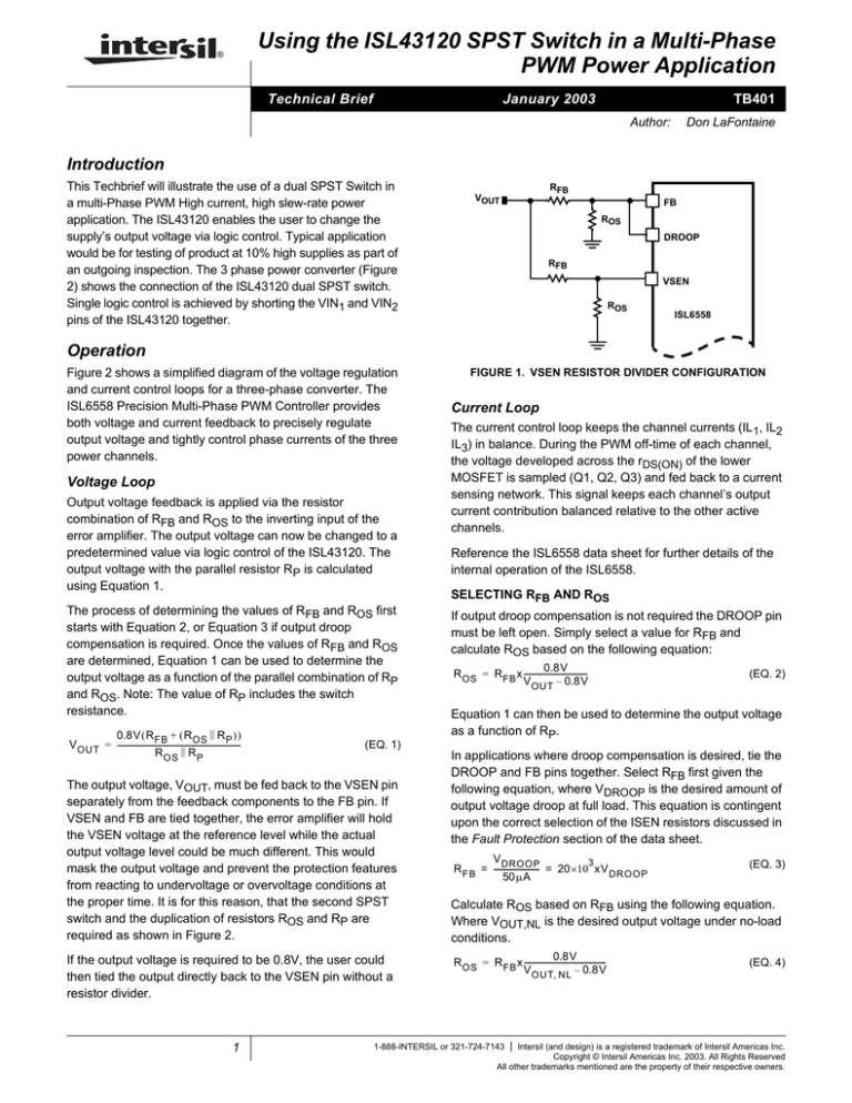
The output voltage, VOUT, must be fed back to the VSEN pin
separately from the feedback components to the FB pin. If
VSEN and FB are tied together, the error amplifier will hold
the VSEN voltage at the reference level while the actual
output voltage level could be much different. This would
mask the output voltage and prevent the protection features
from reacting to undervoltage or overvoltage conditions at
the proper time. It is for this reason, that the second SPST
switch and the duplication of resistors ROS and RP are
required as shown in Figure 2.
If the output voltage is required to be 0.8V, the user could
then tied the output directly back to the VSEN pin without a
resistor divider.
1
FIGURE 1. VSEN RESISTOR DIVIDER CONFIGURATION
In applications where droop compensation is desired, tie the
DROOP and FB pins together. Select RFB first given the
following equation, where VDROOP is the desired amount of
output voltage droop at full load. This equation is contingent
upon the correct selection of the ISEN resistors discussed in
the Fault Protection section of the data sheet.
V DROOP
3
- = 20 ×10 xV DROOP
R FB = -----------------------50µA
(EQ. 3)
Calculate ROS based on RFB using the following equation.
Where VOUT,NL is the desired output voltage under no-load
conditions.
0.8V
R OS = R FB x -------------------------------------------– 0.8V
V
OUT, NL
1-888-INTERSIL or 321-724-7143
|
(EQ. 4)
Intersil (and design) is a registered trademark of Intersil Americas Inc.
Copyright © Intersil Americas Inc. 2003. All Rights Reserved
All other trademarks mentioned are the property of their respective owners.
Technical Brief 401
Typical Application - 3 Phase Converter
VOUT = 0.8V(RFB + ROS || RP)/ ROS || RP
+12V
+5V
RC
+5V
BOOT
IL1
PVCC
UGATE
CC
VCC
RFB
FB
DROOP
+
0.8V
ROS
RP
PHASE
COMP
DRIVER
HIP6601B
PWM
VCC
Q1
LGATE
ERROR
AMPLIFIER
RISEN3
GND
RFB
VOUT
PWM4
PWM3
+12V
VSEN
PWM2
LOGIC
CONTROL
+5V
ROS
BOOT
PWM1
PVCC
PWM
CONTROL
ISL6558
RP
PHASE
ISEN4
PGOOD
ISEN3
FS/EN
NC
VCC
PWM
DRIVER
HIP6601B
ISEN2
RT
GND
IL2
UGATE
LGATE
Q2
RISEN2
GND
ISEN1
+12V
+5V
BOOT
PVCC
PHASE
VCC
PWM
IL3
UGATE
DRIVER
HIP6601B
Q3
LGATE
RISEN1
GND
FIGURE 2. SCHEMATIC OF THE ISL6558 3 PHASE CONVERTER WITH VARIABLE OUTPUT VOLTAGE VIA LOGIC CONTROL
All Intersil U.S. products are manufactured, assembled and tested utilizing ISO9000 quality systems.
Intersil Corporation’s quality certifications can be viewed at www.intersil.com/design/quality
Intersil products are sold by description only. Intersil Corporation reserves the right to make changes in circuit design, software and/or specifications at any time without
notice. Accordingly, the reader is cautioned to verify that data sheets are current before placing orders. Information furnished by Intersil is believed to be accurate and
reliable. However, no responsibility is assumed by Intersil or its subsidiaries for its use; nor for any infringements of patents or other rights of third parties which may result
from its use. No license is granted by implication or otherwise under any patent or patent rights of Intersil or its subsidiaries.
For information regarding Intersil Corporation and its products, see www.intersil.com
2


