TQP887052 Application Note
Application Note for TQP887052 5GHz 802.11a/n/ac FEM MMIC
TQP887052
TABLE OF CONTENTS
1.0 Description
2.0 Product Block Diagram and Operation
3.0 Recommended Handset Schematic and
Layout Considerations
3.1 DC Block Recommendations
3.2 Bypassing Recommendations
3.3 PC Board Layout
4.0 Pin Out Table
5.0 Application Board Information
6.0 Additional Supporting Data
7.0 Additional Information
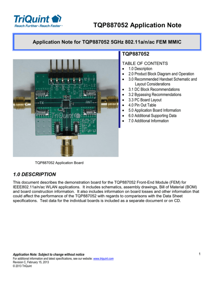
TQP887052 Application Board
1.0 DESCRIPTION
This document describes the demonstration board for the TQP887052 Front-End Module (FEM) for
IEEE802.11a/n/ac WLAN applications. It includes schematics, assembly drawings, Bill of Material (BOM)
and board construction information. It also includes information on board losses and other information that
could affect the performance of the TQP887052 with regards to comparisons with the Data Sheet
specifications. Test data for the individual boards is included as a separate document or on CD.
Application Note: Subject to change without notice
For additional information and latest specifications, see our website: www.triquint.com
Revision C, February 15, 2013
© 2013 TriQuint
1
TQP887052 Application Note
Application Note for TQP887052 5GHz 802.11a/n/ac FEM MMIC
2.0 Product Block Diagram and Operation
Please note that the Product Block Diagram presented here is for reference and discussion purposes and
may not reflect the most up to date version included in the data sheet. Please refer to the data sheet
document from the TriQuint web page for the most up to date information.
PAEN
TX
SW_CTL
PA
ANT
RX
The TQP887052 combines many of the discrete components required for WLAN transmit and receive
chains into a single module. The module contains a Power Amplifier (PA) and RF switch.
The RF ports of the device are TX, ANT and RX. Each of these ports has been internally matched to 50
Ohms. However, some external matching may be required at each of the RF ports to optimize the overall
system performance due to mismatch between the TQP887052 and the RF components following these
ports.
DC supplies and control signals for the PA are carried on VCC1, VCC2, and Vbat, SW_CTL and PAEN.
The VCC pins provide the primary DC power supply for the PA. VCC1 provides DC supply pin of 1 and 2nd
stage of PA, VCC2 is DC supply pin of 3rd stage of PA and Vbias provides DC supply of logic and switch,
while PAEN enables operation of the PA.
In normal operation, TX is connected to the RF output of a SoC. The manufacturer’s recommended
matching network should be used so that the VSWR interaction between the TQP887052 and the SoC is
minimized. The ANT port is connected to the handset antenna. The RX port is connected to the RX input of
the SoC. Again, some matching adjustment may be necessary to get optimum performance from the
complete TX and RX chain.
VCC and Vbat lines are connected directly to the main power supply (battery or DC to DC converter). The
SoC provides SW_CTL and PAEN.
Please refer to the TQP887052 datasheet for further technical specifications.
Application Note: Subject to change without notice
For additional information and latest specifications, see our website: www.triquint.com
Revision C, February 15, 2013
© 2013 TriQuint
2
TQP887052 Application Note
Application Note for TQP887052 5GHz 802.11a/n/ac FEM MMIC
3.0 Recommended Handset Level Schematic and Layout Considerations
The recommended handset level schematic for the TQP887052 is presented in this section. One bypass
capacitors are required on Vbat and two on VCC1/2. These bypass capacitors should be placed as close to
the FEM as possible to reduce supply line inductance.
3.1 DC Block Recommendations
There is no external DC blocking capacitor for all RF ports (Internally DC blocked).
3.2 Bypassing Recommendations
The supply voltage for the FEM is supplied externally through VCC1/2 and Vbat. Power supply bypassing
on VCC1/2 and Vbat is accomplished by 3 surface mount capacitors (C1, C2, C3) and are placed as close
to the FEM as possible. The control voltages are supplied externally though SW_CTL and PAEN. These
pins do not require bypass capacitors but adding provisions for debug purposes is recommended. Values
of the capacitors on control supply lines can be changed to meet dynamic switching speed requirement
Application Note: Subject to change without notice
For additional information and latest specifications, see our website: www.triquint.com
Revision C, February 15, 2013
© 2013 TriQuint
3
TQP887052 Application Note
Application Note for TQP887052 5GHz 802.11a/n/ac FEM MMIC
during initial product development.
3.3 PC Board Layout
3.3.1 RF Layout and Calibration Losses
RF layout is critical in achieving the specified performance of the TQP887052. Impedances of all the RF
traces should be 50 . When determining device performance at the package pins using a connectorized
PC board, the RF trace losses need to be subtracted from the measured data (Section 6.2).
3.3.2 Grounding Considerations
Providing the FEM with proper grounding is required to ensure optimal performance. It is important to
maintain a solid/uninterrupted ground beneath the FEM and ensure the ground vias connect to “True
Ground”. Depending on the type of design, the location of “True Ground” can be different. Do not run
signal traces or supply lines beneath the FEM ground. Below are high level descriptions of two different
designs – Module and Mobile Device PCB:
Module Based Design
In a “Module Based Design”, the WLAN System (FEM and SoC) is mounted on a separate PCB which is
then mounted onto the final product (Mobile Device PCB). The FEM on the module will not see a “True
Ground” until the ground vias make contact to the ground layer of the Mobile Device PCB as illustrated
below.
FEM Ground VIAs
Bypass Caps and Ground Slug
Uninterrupted Connection to Module Bottom Layer
SoC
Module Mid Layer Ground
Not a “True Ground”
FEM
Module Bottom Layer Ground is
Considered to be “True Ground”
Connection Point to Mobile Device PCB
WiFi Radio Module
PCB
Mobile
Device
PCB
Mobile Device PCB Grounds
Depending on Design - May be
Middle layer or Bottom Layer
Mobile Device PCB Design
In a “Mobile Device PCB Design”, the WLAN System is mounted directly onto the final product (Mobile
Device PCB). The FEM will see a “True Ground” when the ground vias connect to the Mobile Device PCB
ground layer.
Application Note: Subject to change without notice
For additional information and latest specifications, see our website: www.triquint.com
Revision C, February 15, 2013
© 2013 TriQuint
4
TQP887052 Application Note
Application Note for TQP887052 5GHz 802.11a/n/ac FEM MMIC
FEM Ground VIAs
Bypass Caps and Ground Slug
Uninterrupted Connection to Mobile Device PCB Ground
SoC
FEM
Mobile Device PCB “True Ground”
Depending on Design - May be
Middle layer or Bottom Layer
WiFi Radio
Mounted Directly
onto Mobile Device
PCB
3.3.3 Footprint Recommendations
This section provides footprint information based on package dimensions. Detailed package dimensions
can be found in the TQP887052 Datasheet.
Top Layer – Metal Layer (in mm)
1.600 +/- 0.050
0.200 +/- 0.050
1.600 +/-0.050
0.475 +/- 0.050
Top Layer – Solder Mask and Stencil (in mm)
Application Note: Subject to change without notice
For additional information and latest specifications, see our website: www.triquint.com
Revision C, February 15, 2013
© 2013 TriQuint
5
TQP887052 Application Note
Application Note for TQP887052 5GHz 802.11a/n/ac FEM MMIC
1.130 +/-0.050
(Square)
1.700 +/- 0.050
0.300 +/- 0.050
1.700 +/-0.050
0.575 +/- 0.050
Solder Stencil:
100% Pad, 50% Ground Slug
Solder Mask
4.0 Pinout Table
Application Note: Subject to change without notice
For additional information and latest specifications, see our website: www.triquint.com
Revision C, February 15, 2013
© 2013 TriQuint
6
TQP887052 Application Note
Application Note for TQP887052 5GHz 802.11a/n/ac FEM MMIC
Application Note: Subject to change without notice
For additional information and latest specifications, see our website: www.triquint.com
Revision C, February 15, 2013
© 2013 TriQuint
7
TQP887052 Application Note
Application Note for TQP887052 5GHz 802.11a/n/ac FEM MMIC
5.0 Application Board Information
The TriQuint Application board has been designed to provide performance as close as possible to the
actual system level performance. Assembly drawings and layer stack up are included here to illustrate
layout practices that will help ensure superior performance in a handset board application. Further
assistance may be requested from TriQuint Application Engineering.
5.1 Application Board Schematic
J4
SW_CTRL
PA_EN
VCC
Vbat
VCC
C12
4.7uF
C11
C7
DNI
C8
DNI
C3
C2
100nF
2.2uF
4.7uF
J1
U1
GND
VCC1
VCC2
NC
J2
R1
GND
ANT
GND
SW_CTL
0
VBAT
GND
RX
GND
TX
GND
PA_EN
GND
C9
PA_EN
SW_CTRL
Vbat
C4
C5
DNI
C10
DNI
TQP887052
C6
DNI
DNI
C1
DNI
100nF
J3
5.2 Applications Board Bill of Material (BOM)
Component
Reference Designator
Value
Size
Quantity
Part Number
FEM
Capacitor
Capacitor
Capacitor
Capacitor
U1
C1,C3
C3
C4
C11,12
0201
0402
0201
0402
1
2
1
1
1
TQP887052
0.1uF
2.2uF
DNI
4.7uF
Application Note: Subject to change without notice
For additional information and latest specifications, see our website: www.triquint.com
Revision C, February 15, 2013
© 2013 TriQuint
8
TQP887052 Application Note
Application Note for TQP887052 5GHz 802.11a/n/ac FEM MMIC
Resistor
Capacitor
R1,
C5,C6,C7,C8,C9,C10
0 Ohm
DNI
Application Note: Subject to change without notice
For additional information and latest specifications, see our website: www.triquint.com
Revision C, February 15, 2013
© 2013 TriQuint
0201
1
9
TQP887052 Application Note
Application Note for TQP887052 5GHz 802.11a/n/ac FEM MMIC
5.3 Application Board Silkscreen and Top Assembly Drawing
Silkscreen
Top Assembly Drawing
Application Note: Subject to change without notice
For additional information and latest specifications, see our website: www.triquint.com
Revision C, February 15, 2013
© 2013 TriQuint
10
TQP887052 Application Note
Application Note for TQP887052 5GHz 802.11a/n/ac FEM MMIC
6.0 Additional Supporting Data
6.1 Truth Table for Various Modes
Application Note: Subject to change without notice
For additional information and latest specifications, see our website: www.triquint.com
Revision C, February 15, 2013
© 2013 TriQuint
11
TQP887052 Application Note
Application Note for TQP887052 5GHz 802.11a/n/ac FEM MMIC
6.2 PC Board Offset
The following are the offsets (5.5GHz) that can be used for the TriQuint application board as mentioned in
section 3.3.1.
MEASUREMENT
OFFSET
RX port Insertion Loss
0.21dB
TX port Insertion Loss
0.25dB
Antenna port Loss
0.25dB
Application Note: Subject to change without notice
For additional information and latest specifications, see our website: www.triquint.com
Revision C, February 15, 2013
© 2013 TriQuint
12
TQP887052 Application Note
Application Note for TQP887052 5GHz 802.11a/n/ac FEM MMIC
7.0 Additional Information
For technical questions and application information: Please contact TriQuint Application Engineering Team
Additional Information
1
1
For latest specifications, additional product information, worldwide sales and distribution locations, and information about TriQuint:
Web: www.triquint.com
Tel: (503) 615-9000
Email: info_wireless@tqs.com
Fax: (503) 615-8902
For technical questions and additional information on specific applications:
Email: info_wireless@tqs.com
The information provided herein is believed to be reliable; TriQuint assumes no liability for inaccuracies or omissions. TriQuint assumes no responsibility for the use of this
information, and all such information shall be entirely at the user's own risk. Prices and specifications are subject to change without notice. No patent rights or licenses to any of the
Application Note: Subject to change without notice
For additional information and latest specifications, see our website: www.triquint.com
Revision C, February 15, 2013
© 2013 TriQuint
13
TQP887052 Application Note
Application Note for TQP887052 5GHz 802.11a/n/ac FEM MMIC
circuits described herein are implied or granted to any third party. TriQuint does not authorize or warrant any TriQuint product for use in life-support devices and/or systems.
Copyright © 2006 TriQuint Semiconductor, Inc. All rights reserved.
Application Note: Subject to change without notice
For additional information and latest specifications, see our website: www.triquint.com
Revision C, February 15, 2013
© 2013 TriQuint
14
